
Display driving circuit, display device and display driving method

A display driver and circuit technology, applied in static indicators, instruments, etc., can solve problems such as difference in charging effect, and achieve the effect of reducing cost and improving display effect.

Inactive Publication Date: 2019-07-05
CHONGQING BOE OPTOELECTRONICS +1
View PDF11 Cites 0 Cited by
  • Summary
  • Abstract
  • Description
  • Claims
  • Application Information

AI Technical Summary

Problems solved by technology

[0003] Aiming at the defects in the prior art, the present invention provides a display driving circuit, a display device and a display driving method, which can solve the problem in the prior art that there are significant differences in charging effects between pixels connected by different rows of gate scanning lines

Method used


Image

  • Display driving circuit, display device and display driving method
  • Display driving circuit, display device and display driving method
  • Display driving circuit, display device and display driving method

Examples


Embodiment Construction

[0033] In order to make the purpose, technical solutions and advantages of the embodiments of the present invention clearer, the technical solutions in the embodiments of the present invention will be clearly and completely described below in conjunction with the drawings in the embodiments of the present invention. Obviously, the described embodiments It is a part of embodiments of the present invention, but not all embodiments. Based on the embodiments of the present invention, all other embodiments obtained by persons of ordinary skill in the art without creative efforts fall within the protection scope of the present invention.

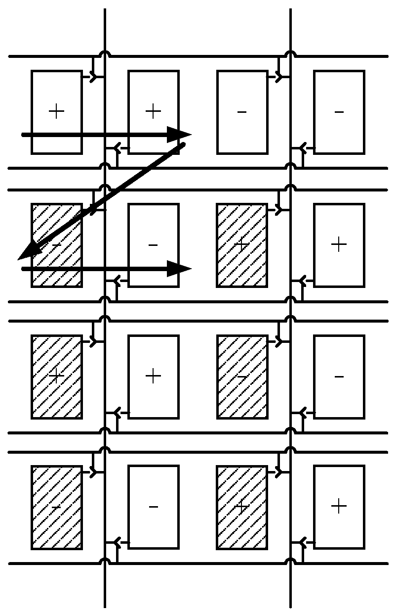
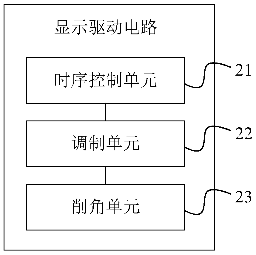
[0034] figure 2 It is a structural block diagram of a display driving circuit in an embodiment of the present invention. see figure 2 , the display drive circuit includes a timing control unit 21, a modulation unit 22 and a chamfering unit 23, wherein:

[0035] The timing control unit 21 is connected to the modulation unit 22, specifically fo...


PUM


Abstract

The present invention provides a display driving circuit, a display device and a display driving method, wherein the display driving circuit includes: a timing control unit, a modulating unit, and a chamfering unit, wherein: the timing controlling unit is connected to the modulating unit, and is used to The signal generates a line selection signal, a first control signal including a chamfer width signal and a chamfer depth signal, and a second control signal including a width modulation signal and / or a depth modulation signal; the modulating unit is connected to the chamfer unit, for according to the first The second control signal modulates the first control signal in the period when the line selection signal is at an effective level; the chamfering unit is used to perform the grid voltage signal according to the first control signal modulated by the modulation unit before outputting the grid voltage signal Chamfered treatment. Based on this, the present invention can solve the problem in the prior art that there is a significant difference in charging effect between pixels connected by different row gate scanning lines, which is beneficial to the improvement of display effect.

Description

technical field [0001] The invention relates to the field of display technology, in particular to a display driving circuit, a display device and a display driving method. Background technique [0002] In the existing liquid crystal display (Liquid Crystal Display, LCD), due to the difference in the arrangement of the pixel electrode array and the type of polarity inversion, there may be significant differences in the charging effect between pixels connected by different row gate scan lines The problem. E.g figure 1 In the prior art shown in a Z inversion charging mode under a double-gate structure, the charging polarities of the data lines in the first column between the pixels in the first two rows are "+", "+", "-", "-". Among them, such as figure 1 As shown by the oblique arrow in , when the charging polarity of the data line in the first column is changed from "+" to "-", the voltage amplitude span is too large and the parasitic capacitance on the data line will mak...

Claims


Application Information

Patent Timeline
Patent Type & Authority Patents(China)
IPC IPC(8): G09G3/36
CPCG09G3/3611G09G3/3674G09G3/3696G09G2310/06G09G2310/08G09G2320/0209G09G2320/0219G09G2320/0233G09G3/36G09G3/3614G09G2310/067
Inventor 陈帅张智伏思庆梁利生高贤永文江鸿钱谦唐秀珠王志会陈磊唐滔良陈刚
Owner CHONGQING BOE OPTOELECTRONICS
Learn More