Contact through hole etching method

A contact through-hole and etching technology, which is applied in the direction of electrical components, semiconductor/solid-state device manufacturing, circuits, etc., can solve problems affecting the CVD process, current leakage, etc., to eliminate notches and high roughness, good shape, and avoid The effect of the potential risk of current leakage

Active Publication Date: 2016-01-13
SEMICON MFG INT (SHANGHAI) CORP
View PDF3 Cites 0 Cited by
  • Summary
  • Abstract
  • Description
  • Claims
  • Application Information

AI Technical Summary

Problems solved by technology

Both the above-mentioned notch and roughness will adversely affect the subsequent CVD process and cause current leakage problems

Method used


Image

  • Contact through hole etching method
  • Contact through hole etching method
  • Contact through hole etching method

Examples


Embodiment Construction

[0026] Embodiments of the present invention will now be described in detail with reference to the accompanying drawings. Reference will now be made in detail to the preferred embodiments of the invention, examples of which are illustrated in the accompanying drawings. Wherever possible, the same numbers will be used throughout the drawings to refer to the same or like parts. In addition, although the terms used in the present invention are selected from well-known and commonly used terms, some terms mentioned in the description of the present invention may be selected by the applicant according to his or her judgment, and the detailed meanings thereof are set forth herein described in the relevant section of the description. Furthermore, it is required that the present invention be understood not only by the actual terms used, but also by the meaning implied by each term.

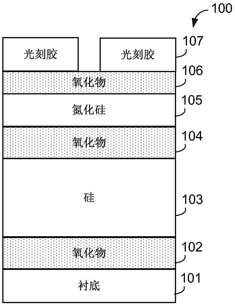
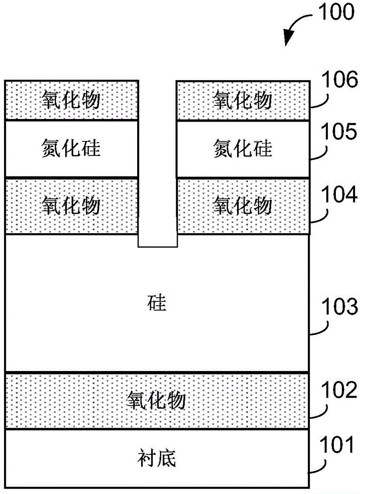
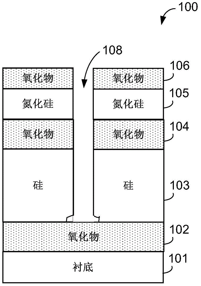
[0027] first reference Figure 2-Figure 3c , which shows a flow chart of the basic steps of the conta...


PUM


Abstract

The invention provides a contact through hole etching method which is applicable to a composite layer structure formed by at least stacking a first material layer and a second material layer, wherein the first material layer and the second material layer are made of different materials. The contact through hole etching method comprises the steps as follows: a, using a Bosch etching process to etch the first material layer to form a contact through hole in the first material layer, wherein the Bosch etching process further comprises the following sub steps: a1, forming a polymer on the side wall and bottom of the contact through hole; a2, removing the polymer on the bottom of the contact through hole; a3, etching the inside of the contact through hole by a predetermined depth; and a4, repeating the sub steps a1 to a3 until the contact through hole reaches a specified depth in the first material layer; and b, using another etching process different from the Bosch etching process to etch the contact through hole reaching the specified depth to enable the contact through hole to extend into the second material layer under the first material layer. By adopting the method of the invention, the contact through hole formed though etching has a better shape.

Description

technical field [0001] The invention relates to the field of manufacturing semiconductor integrated circuit devices, in particular to a contact through hole etching method. Background technique [0002] With the deepening of technological development, the feature size of semiconductor devices has become very small now, and it is becoming more and more difficult to increase the number of semiconductor devices in a two-dimensional packaging structure. Therefore, three-dimensional packaging has become a method that can effectively improve chip integration. degree method. Current three-dimensional packaging includes gold wire bonding-based chip stacking (DieStacking), package stacking (PackageStacking), and through-silicon via (ThroughSiliconVia, TSV)-based three-dimensional stacking. Among them, the three-dimensional stacking technology using through-silicon vias has the following three advantages: (1) high-density integration; (2) greatly shortening the length of electrical i...

Claims


Application Information

Patent Timeline
Patent Type & Authority Applications(China)
IPC IPC(8): H01L21/768
Inventor 伏广才许继辉苏良得倪梁汪新学
Owner SEMICON MFG INT (SHANGHAI) CORP
Why Eureka
Try Eureka