Pixel sensor device and operating method thereof

A technology of a sensing device and an operation method, applied in image communication, TV system components, TV, etc., can solve problems such as difficult focusing, inconvenient use, inaccurate measurement, etc., and achieve the effect of improving accuracy

Inactive Publication Date: 2016-03-02
ELAN MICROELECTRONICS CORPORATION
View PDF5 Cites 6 Cited by
  • Summary
  • Abstract
  • Description
  • Claims
  • Application Information

AI Technical Summary

Problems solved by technology

[0004] For the above-mentioned electronic device integrating two or more different optical applications, two different sensing elements must be used, such as the active pixel sensing array element 601 and the light sensing element 701, and the two sensing elements use different The circuit design is not ideal in terms of cost and size, and in terms of dual applications of fingerprint recognition and pulse measurement, users need to place their fingers on different sensing elements, which is inconvenient to use
[0005] In addition, since the active pixel sensing array element 601 and the light sensing element 701 of this dual-application optical sensing device are formed in different regions, if only a single focusing element is used, the active pixel sensing array element 601 or when focusing on the light sensing element 701, because it is not directly aimed at a single area, it will be difficult to focus and have the problem of inaccurate measurement; if two focusing elements are used for the active pixel sensing array element 601 and the The light sensing element 701 is used for focusing, which will make the cost higher and the control circuit more complicated

Method used


Image

  • Pixel sensor device and operating method thereof
  • Pixel sensor device and operating method thereof
  • Pixel sensor device and operating method thereof

Examples


Embodiment Construction

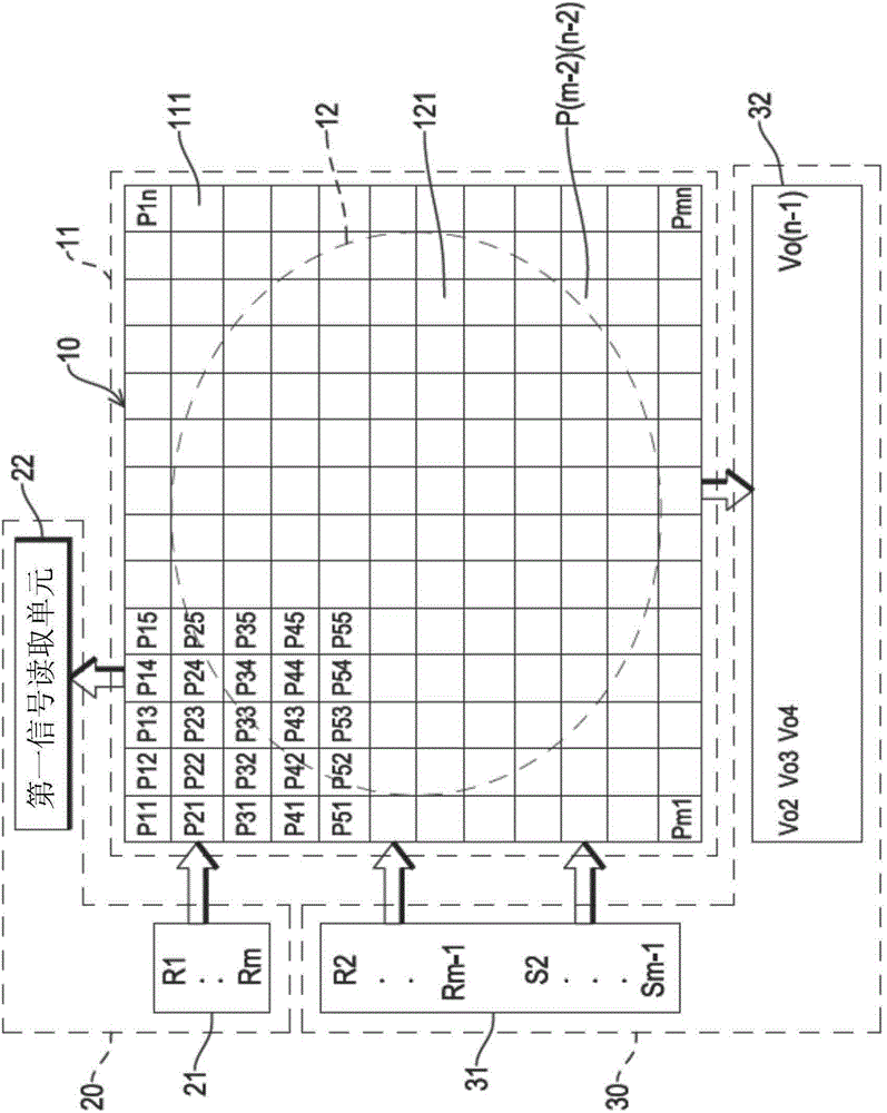
[0080] The present invention proposes a pixel sensing device capable of partitioning sensing, which is designed by using a single pixel sensing array element, so that it can support different applications separately or simultaneously, and will be described in several embodiments below.

[0081] See first Figure 1A As shown, the pixel sensing device of the present invention that can sense partitions includes a first sensing unit 11, a second sensing unit 12, a first control and read unit 20, and a second control and read unit 30 .

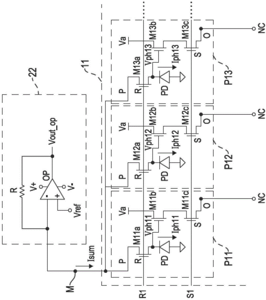
[0082] The above-mentioned first and second sensing units 11, 12 are composed of a single pixel sensing array element 10, wherein the first sensing unit 11 includes a plurality of first sensing pixels 111 arranged in a ring (such as a white square ), and the second sensing unit 12 also includes a plurality of second sensing pixels 121 (shown in gray squares), and all the first sensing pixels 111 are arranged in a ring on the second sensing unit 12...


PUM


Abstract

A pixel sensor device has a first sensing unit, a second sensing unit, a first control and reading unit, and a second control and reading unit. The first and second sensing units are disposed concentrically. The first and second control and reading units are connected respectively to the first and second sensing units for separately or simultaneously controlling the first and second sensing units to perform sensing. Since the first and second sensing units are formed by a single pixel sensing array and arranged concentrically, only a single focusing element is required to align centers of the first and second sensing units during the manufacturing process. This achieves high focus accuracy and increases precision in recognition. In the applications of fingerprint recognition and pulse measurement, the user only uses a single finger for sensing so that inaccurate focusing resulted from moving finger is avoided.

Description

technical field [0001] The present invention relates to an active pixel sensing device and an operating method thereof, in particular to a partitionable sensing pixel sensing device and an operating method thereof. Background technique [0002] Currently, there are two types of optical sensing devices used in fingerprint recognition. One is a passive pixel sensor (Passive Pixel Sensor, PPS), and the other is an active pixel sensor (Active Pixel Sensor, APS). Regardless of the passive or active pixel sensing device, when sensing the fingerprint, each sensing pixel is reset and then exposed, and then the sensing current is read and converted into a corresponding sensing voltage. However, in addition to the fingerprint recognition function, there are also many optical sensing applications, such as: ambient light sensing or pulse detection, where the pulse detection is obtained by detecting the changes in the contraction and relaxation of the microvessels, the resolution require...

Claims


Application Information

Patent Timeline
Patent Type & Authority Applications(China)
IPC IPC(8): G06K9/00G06V40/13
CPCG06V40/13H04N25/42H04N25/702H04N25/75
Inventor 吴伯豪刘醇铠
Owner ELAN MICROELECTRONICS CORPORATION
Why Eureka
Try Eureka