PCB package library structure and packaging method

A packaging method and packaging library technology, which is applied to the assembly of printed circuits with electrical components, electrical components, and printed circuit manufacturing, and can solve problems such as unsafe hidden dangers, fires, and products that cannot be released on time

Inactive Publication Date: 2016-03-23
GUANGDONG VTRON TECH CO LTD
View PDF3 Cites 0 Cited by
  • Summary
  • Abstract
  • Description
  • Claims
  • Application Information

AI Technical Summary

Problems solved by technology

[0005] The embodiment of the present invention provides a PCB packaging library structure and packaging method, which solves the short circuit of the PCB caused by wave soldering, which can cause a short circuit in the PCB, burn out the PCB, and cause the product to not be released on time, or cause the short circuit to cause the PCB to catch fire. Technical problems that cause fires, resulting in unsafe hazards

Method used


Image

  • PCB package library structure and packaging method
  • PCB package library structure and packaging method
  • PCB package library structure and packaging method

Examples


Embodiment Construction

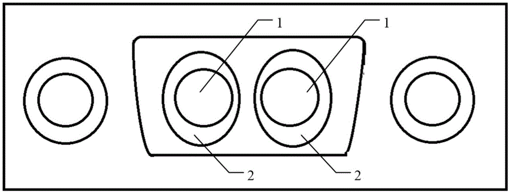
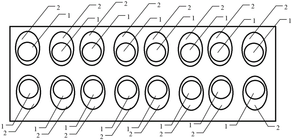
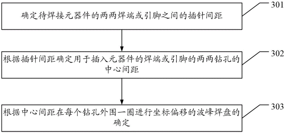
[0033] The embodiment of the present invention provides a PCB packaging library structure and packaging method, which solves the short circuit of the PCB caused by wave soldering, which may cause a short circuit in the PCB, burn out the PCB, and cause the product to not be released on time, or cause a fire in the PCB caused by a short circuit. Technical problems that cause fires and lead to unsafe hidden dangers.

[0034] In order to make the purpose, features and advantages of the present invention more obvious and understandable, the technical solutions in the embodiments of the present invention will be clearly and completely described below in conjunction with the accompanying drawings in the embodiments of the present invention. Obviously, the following The described embodiments are only some, not all, embodiments of the present invention. Based on the embodiments of the present invention, all other embodiments obtained by persons of ordinary skill in the art without maki...


PUM


Abstract

Embodiments of the present invention disclose a PCB package library structure and a packaging method, and solve the technical problem of unsafe hidden dangers caused by the case that due to continuous tin short circuiting of wave soldering, PCB short circuiting is caused and a PCB is burnt out so as to enable a product not to be released on time, and even short circuiting is caused and the PCB is on fire to cause a fire disaster . The PCB package library structure disclosed by the embodiments of the present invention comprises a plurality of drill holes for inserting welding ends or pins of components, wherein a circle of coordinate deviated wave peak bonding pad is arranged on the periphery of each drill hole; and a distance between the wave peak bonding pads between the peripheries of every two adjacent drill holes is not less than 1 mm.

Description

technical field [0001] The invention relates to the technical field of electronic circuits, in particular to a PCB package library structure and a package method. Background technique [0002] With the rapid development of electronic products in recent years, the demand for high current on printed circuit boards is increasing. Many single boards use power connectors to input and output power, and the high-current connectors generally used in the industry are plug-in pin connector. [0003] Therefore, it is necessary to solder by wave soldering. Wave soldering refers to the molten solder (lead-tin alloy), which is sprayed by an electric pump or an electromagnetic pump into a solder wave peak required by the design, or by injecting nitrogen into the solder pool. It is formed to make the printed board pre-installed with components pass through the solder wave to realize the soldering of the mechanical and electrical connection between the component soldering end or the pin and...

Claims


Application Information

Patent Timeline
Patent Type & Authority Applications(China)
IPC IPC(8): H05K3/34
CPCH05K3/3447H05K2203/1316
Inventor 刘海龙
Owner GUANGDONG VTRON TECH CO LTD
Why Eureka
Try Eureka