Novel gate structure and manufacture method thereof

A manufacturing method and technology of gate structure, which can be applied to electrical components, circuits, semiconductor devices, etc., and can solve problems such as device damage, device turn-on delay, and large delay.

Pending Publication Date: 2016-03-30
GLOBAL ENERGY INTERCONNECTION RES INST CO LTD +2
View PDF6 Cites 2 Cited by
  • Summary
  • Abstract
  • Description
  • Claims
  • Application Information

AI Technical Summary

Problems solved by technology

[0002] At present, the gate structure in semiconductor power devices usually adopts the design of a single pad ring peripheral bus bar. This structural design has the following disadvantages: when the device is turned on, the gate voltage is first applied to the gate pad, and then conducted to the surrounding

Method used


Image

  • Novel gate structure and manufacture method thereof

Examples


Embodiment 1

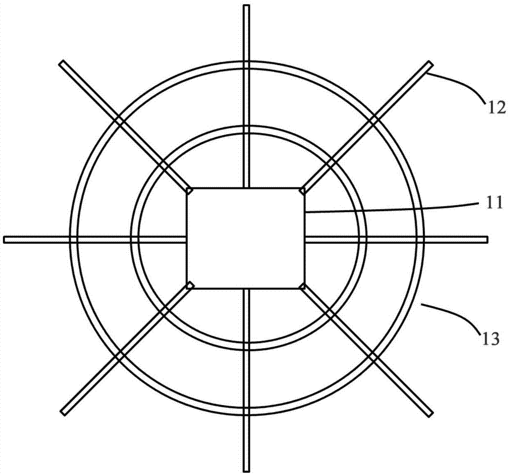
[0021] A novel grid structure includes a grid pad area 11, a radial bus bar 12 emanating from the grid pad area 11, an annular bus bar 13 surrounding the grid pad area 11, and the radial bus bar 12 and the annular bus bar 13 The intersection point is connected to the surrounding cell grid; the number of the radial bus bars is 8, and the width is 20 μm; the number of the ring bus bars is 2, the width of the bus bars is 20 μm, and the distance from the grid pad is relatively close The diameter of the ring is 800 μm, and the diameter of the ring farther from the grid pad is 2000 μm; the structure is as shown figure 1 As shown; the gate pad region 11, the emissive bus bar 12, and the annular bus bar 13 are made of n-type degenerately doped polysilicon.

[0022] The specific manufacturing method of the new gate structure is as follows:

[0023] 1) drawing the layout of the grid pad region 11, the emissive bus bar 12 and the annular bus bar 13 on the same layer;

[0024] 2) prepar...

Embodiment 2

[0027] A novel grid structure includes a grid pad area 11, a radial bus bar 12 emanating from the grid pad area 11, an annular bus bar 13 surrounding the grid pad area 11, and the radial bus bar 12 and the annular bus bar 13 The intersection point is connected with the surrounding cell grid; the number of the radial bus bars is 10, and the width is 18 μm; the number of the ring bus bars is 3, the width of the bus bars is 15 μm, and the diameter of the ring is successively 800μm, 1500μm, 2500μm; structure as shown figure 1 As shown; the gate pad area 11, the emissive bus bar 12, and the annular bus bar 13 are prepared from a single metal layer of Ag.

[0028] The specific manufacturing method of the new gate structure is as follows:

[0029] 1) drawing the layout of the grid pad region 11, the emissive bus bar 12 and the annular bus bar 13 on the same layer;

[0030] 2) deposit and prepare the Ag metal layer of the gate pad region 11, the emissive bus bar 12 and the annular b...

Embodiment 3

[0033] A novel grid structure includes a grid pad area 11, a radial bus bar 12 emanating from the grid pad area 11, an annular bus bar 13 surrounding the grid pad area 11, and the radial bus bar 12 and the annular bus bar 13 The intersection point is connected with the surrounding cell grid; the number of the radial bus bars is 15, and the width is 15 μm; the number of the ring bus bars is 5, the width of the bus bars is 15 μm, and the diameter of the ring is successively 800μm, 1500μm, 2500μm, 3500μm, 4500μm; structure as shown figure 1 As shown; the gate pad area 11, the emissive bus bar 12, and the annular bus bar 13 are prepared from a single metal layer of Ag.

[0034] The specific manufacturing method of the new gate structure is as follows:

[0035] 1) drawing the layout of the grid pad region 11, the emissive bus bar 12 and the annular bus bar 13 on the same layer;

[0036] 2) depositing and preparing a composite metal layer of Ag and Al in the grid pad region 11, th...


PUM

PropertyMeasurementUnit
Widthaaaaaaaaaa
Diameteraaaaaaaaaa

Abstract

The invention discloses a novel gate structure and a manufacture method thereof. The gate structure comprises a gate pad area (11) with electrode leads, radial bus bars (12) and annular bus bars (13), wherein the gate pad area (11), the radial bus bars (12) and the annular bus bars (13) are arranged on the same plane; the radial bus bars (12) take the gate pad area (11) as the center; and the radial bus bars (12) and the annular bus bar (13) are connected with a surrounding cellular gate. The method comprises the following steps: drawing a domain of the gate pad area (11), the radial bus bars (12) and the annular bus bars (13) on the same layer; preparing the gate pad area (11), the radial bus bars (12) and the annular bus bars (13); and preparing the electrode leads on the gate pad area (11), and isolating the radial bus bars (12) and the annular bus bars (13) from a source electrode or other through-flow electrodes. The reticular bus bars of the gate structure are favorable for expanding gate voltage, and the problem of open delay of cells far away from the gate pad due to gate voltage expansion delay is alleviated so as to improve the stability of device performance.

Description

technical field [0001] The invention relates to the technical field of semiconductors, in particular to a novel gate structure and a manufacturing method thereof. Background technique [0002] At present, the gate structure in semiconductor power devices usually adopts the design of a single pad ring peripheral bus bar. This structural design has the following disadvantages: when the device is turned on, the gate voltage is first applied to the gate pad, and then conducted to the surrounding area directly connected to the gate pad. On the cellular grid and the bus bar, a large delay is usually generated when the gate voltage is transmitted to the cellular grid far away from the gate pad. This delay will lead to a delay in the turn-on of the device, unstable performance, and even damage to the device. Contents of the invention [0003] The purpose of the present invention is to provide a novel grid structure and its manufacturing method. The mesh bus bar of the grid structu...

Claims


Application Information

Patent Timeline
IPC IPC(8): H01L29/423H01L21/28
CPCH01L29/401H01L29/42312
Inventor 杨霏郑柳王方方朱韫晖吴昊王嘉铭
Owner GLOBAL ENERGY INTERCONNECTION RES INST CO LTD
Why Eureka
Try Eureka