A kind of led potting device

An LED chip, potting technology, applied in the direction of electrical components, circuits, semiconductor devices, etc., can solve problems such as incompatibility, and achieve the effects of reducing production costs, strong technical operability, and simple process

Active Publication Date: 2018-01-26
合肥新观点照明科技股份有限公司
View PDF6 Cites 0 Cited by
  • Summary
  • Abstract
  • Description
  • Claims
  • Application Information

AI Technical Summary

Problems solved by technology

However, this method is not suitable for LED devices with integrated lens structure. In order to make it easy to complete through the simple process of dieless dispensing, there is an urgent need for a new structure of LED devices.

Method used


Image

  • A kind of led potting device

Examples


Embodiment Construction

[0011] The present invention will be further described below in conjunction with the accompanying drawings.

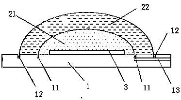
[0012] Such as figure 1 As shown, the LED potting device of this embodiment includes a substrate 1, an LED chip 3 mounted on the substrate 1, and a lens wrapped outside the LED chip 3. The lens includes a base layer 21 wrapped outside the LED chip 3 and a cover The stacked layer 22 is formed outside the base layer 21. On the substrate 1 and at the outer edges of the base layer 21 and the stacked layer 22, a first annular groove 11 and a second annular groove 12 are respectively provided. The first annular groove 11 and the outer edge of the stacked layer 22 are respectively provided with The second annular grooves 12 communicate with each other through the drain groove 13 , and the drain port of the drain groove 13 protrudes from the side wall of the substrate 1 ; the stacking layer 22 is composed of multiple layers of encapsulation glue. The base layer 21 adopts a pl...


PUM


Abstract

The invention relates to a light emitting diode (LED) encapsulating device. The LED encapsulating device comprises a base plate, an LED chip and a lens, wherein the LED chip is arranged on the base plate, the lens wraps the LED chip and comprises a basic layer and a stack layer, the basic layer wraps the LED chip, the stack layer covers the basic layer, a first annular groove and a second annular groove are respectively arranged on the base plate and at outer edges of the basic layer and the stack layer and communicated with each other via a liquid discharge groove, and a liquid discharge hole of the liquid discharge groove extends from the side wall of the base plate. With the LED encapsulating device, wafer level package of an LED can be achieved in no need of a die, the technological operability is high, the process is simple, and the production cost of the LED also can be reduced.

Description

technical field [0001] The invention belongs to the technical field of LED encapsulation, and in particular relates to an LED encapsulation device. Background technique [0002] Due to the advantages of power saving, long life and small size, LED lamps have been increasingly used in lighting, backlighting and other fields, and are expected to replace traditional light sources such as incandescent lamps and fluorescent lamps. The traditional packaging process of LED devices is a device-level process, which has high cost and is difficult to perform high-density packaging. The lenses of the existing LED devices basically adopt an integrated structure of one-time molding. Most of the traditional lens packages use prefabricated lenses or mold molding methods, which are not suitable for wafer-level packaging. [0003] Based on this, people hope to use the moldless dispensing process to package the lens of the wafer-level LED chip. The simplest and intuitive method of moldless dis...

Claims


Application Information

Patent Timeline
Patent Type & Authority Patents(China)
IPC IPC(8): H01L33/48H01L33/52H01L33/56
CPCH01L33/483H01L33/52H01L33/56
Inventor 高伟冯世
Owner 合肥新观点照明科技股份有限公司
Why Eureka
Try Eureka