Wafer-level packaging sensibilization and noise reduction structure of miniature electric field sensor

An electric field sensor, wafer-level packaging technology, applied in microelectronic microstructure devices, microstructure technology, microstructure devices and other directions, can solve problems such as complex process flow, improve noise reduction performance, increase output induced current, Simple and effective manufacturing process

Pending Publication Date: 2022-03-25
AEROSPACE INFORMATION RES INST CAS +1
View PDF0 Cites 0 Cited by
  • Summary
  • Abstract
  • Description
  • Claims
  • Application Information

AI Technical Summary

Problems solved by technology

[0005] In the wafer-level packaging scheme based on bonding, the electrical signals in the sealed cavity need to be drawn out horizontally through planar electrodes or vertically through TSV electrodes. more complex issues
In addition, if substrate grounding is required, additional process steps need to be added, and additional pads or metal leads need to be made

Method used


Image

  • Wafer-level packaging sensibilization and noise reduction structure of miniature electric field sensor
  • Wafer-level packaging sensibilization and noise reduction structure of miniature electric field sensor
  • Wafer-level packaging sensibilization and noise reduction structure of miniature electric field sensor

Examples


Embodiment 1

[0050] The manufacturing process steps of a miniature electric field sensor wafer-level package sensitivity-increasing and noise-reducing structure of the present disclosure are as follows.

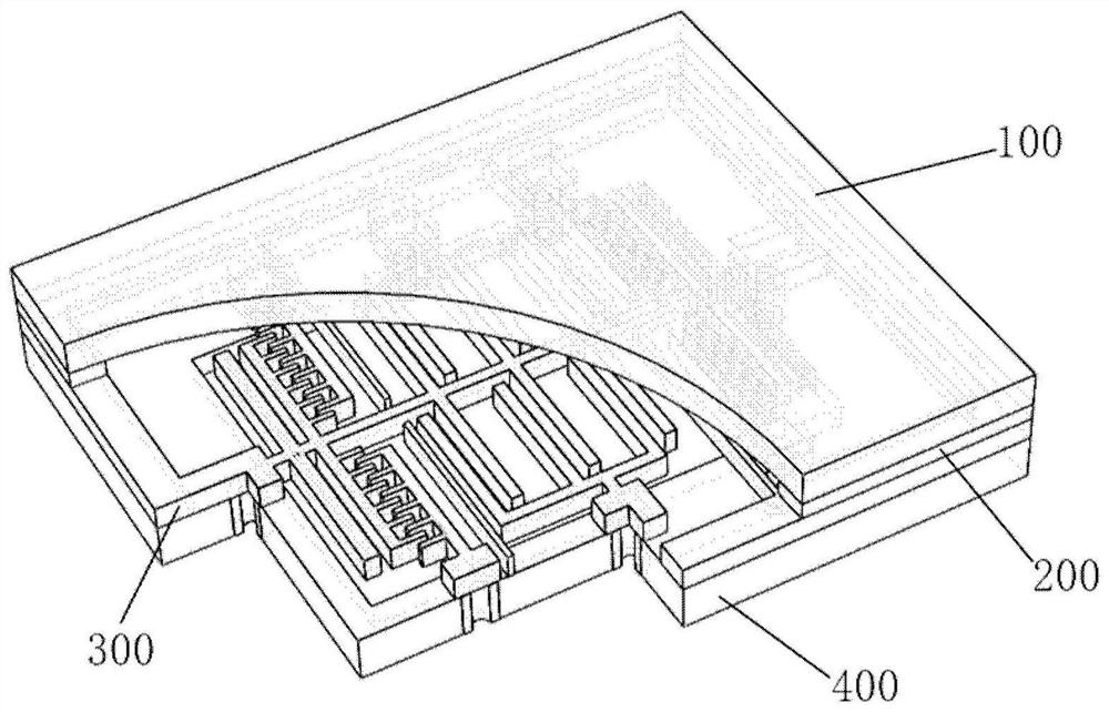
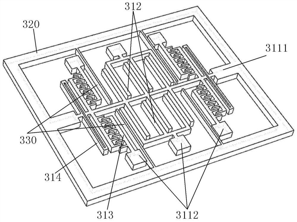
[0051] refer to Figure 4 , using the supporting layer of the SOI wafer as the capping layer 100, the structural silicon layer and the buried oxide layer of the SOI wafer are sequentially processed into the device layer 300 and the second insulating layer 200, including: the structure of an SOI wafer The first anchor point 3111, the second anchor point 3112, the sensing structure 312, the driving structure 313, the elastic beam 314, the rectangular closed sealing ring 320 and the shielding beam 330 are etched on the silicon layer to obtain the device layer 300; the release and rectangular sealing ring In the rectangular area corresponding to the inner circle of 320, and removing the buried oxide layer except the positions corresponding to the first anchor point 3111 and the second anchor ...

Embodiment 2

[0055] The preparation steps of another miniature electric field sensor wafer-level packaging sensitivity-increasing and noise-reducing structure of the present disclosure are as follows.

[0056] In this embodiment, the methods for preparing the device layer 300 , the second insulating layer 200 , and the capping layer 100 are the same as those in the first embodiment.

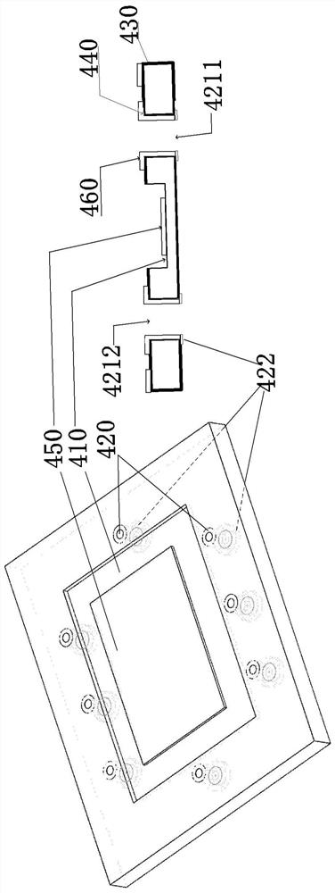
[0057] refer to Figure 7 , etch a groove 410 on a conductive silicon wafer to obtain a base layer 400; grow a first insulating layer 430 on the upper surface of the base layer 400; The window 440 is etched at the position corresponding to the point 3112; the bonding dielectric layer 460 is grown on the position corresponding to the rectangular closed sealing ring 320, the first anchor point 3111, and the second anchor point 3112 of the device layer 300 on the first insulating layer 430, Wherein, the bonding medium layer 460 covers the window 440 on the first insulating layer 430 ; a thin layer of getter 450 i...

Embodiment 3

[0060] On the basis of the second embodiment, this embodiment provides another method for fabricating the vertical interconnection structure 420 .

[0061] In this embodiment, as in Embodiment 2, refer to Figure 4 The method shown prepares the device layer 300, the second insulating layer 200, and the capping layer 100; as in the second embodiment, refer to Figure 7 The method shown prepares the base layer 400 , the first insulating layer 430 , the bonding medium layer 460 , and the thin layer of the getter 450 , and the like.

[0062] refer to Figure 9 First, as in Example 2, in a vacuum environment, the rectangular closed sealing ring 320, the first anchor point 3111, and the second anchor point 3112 prepared on the SOI wafer are bonded to the prepared conductor silicon wafer, At the same time, the activation of the getter 450 is completed; then, silicon is etched at the corresponding positions of the first anchor point 3111 and the second anchor point 3112 at the botto...


PUM


Abstract

A micro electric field sensor wafer level packaging sensitization and noise reduction structure is mainly composed of three layers of wafer level conductor silicon and two layers of insulating materials, and comprises a substrate layer provided with a groove and a plurality of vertical interconnection structures, a first insulating layer deposited on the surface, and a second insulating layer deposited on the surface; the substrate layer is connected and grounded with the grounding vertical interconnection structure through an etching window on the first insulating layer, so that coupling crosstalk noise is reduced; a sensing structure, a closed sealing ring and a shielding beam are etched on the device layer, and coupling noise in the device layer is reduced by the grounding shielding beam; the sealing cap layer is insulated from the device layer through the second insulating layer, and a tiny gap is formed between the hollow area of the second insulating layer and the sensing structure, so that the intensity of an electric field around the sensing structure is enhanced, and the sensitivity of the sensor is improved. The wafer level packaging of the electric field sensor can be realized, the characteristics of sensitization and noise reduction are realized, and the manufacturing process is simple.

Description

technical field [0001] The present disclosure relates to the technical field of sensor manufacturing, in particular to a wafer-level package sensitivity enhancement and noise reduction structure for a miniature electric field sensor. Background technique [0002] Electric field sensor is a device for detecting electric field strength, which is widely used in meteorological detection, aerospace, petrochemical, electric power and many other fields. Micro electric field sensors based on MEMS technology have become a research hotspot and development direction of electric field sensors due to their small size, low cost, and mass production. At present, the miniature electric field sensor has problems such as small output signal, low signal-to-noise ratio, and small Q value, which restrict its application and development. [0003] The existing miniature electric field sensor packaging structure needs to be mounted and sealed one by one, which is not conducive to mass production. ...

Claims


Application Information

Patent Timeline
Patent Type & Authority Applications(China)
IPC IPC(8): B81B7/02B81B7/00B81C1/00G01R29/12
CPCG01R29/12B81B7/02B81B7/0064B81B7/007B81C1/00301B81C1/00269B81B2201/0292
Inventor 夏善红刘俊储昭志雷虎成彭春荣
Owner AEROSPACE INFORMATION RES INST CAS
Why Eureka
Try Eureka