

Wafer level packaging structure of chip, and preparation method of wafer level packaging structure
A wafer-level packaging and chip technology, applied in electrical components, circuits, semiconductor devices, etc., to overcome chip short-circuits, improve welding strength and sealing effect
- Summary
- Abstract
- Description
- Claims
- Application Information
AI Technical Summary
Problems solved by technology
Method used
Image

Examples
Embodiment 1
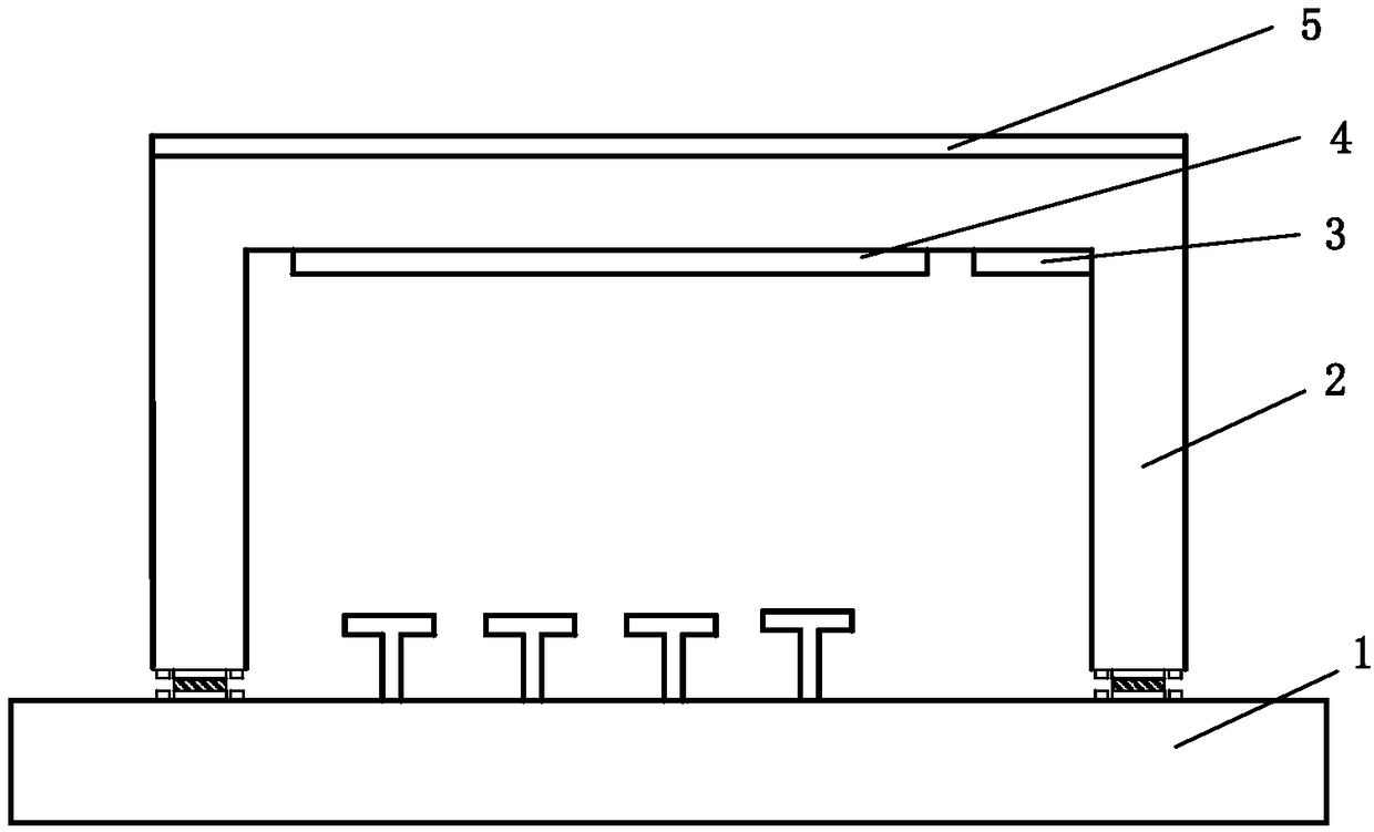
[0036] This embodiment provides a chip wafer-level packaging structure, including a chip 1, and also includes a vacuum cavity structure, and the vacuum cavity structure encapsulates the chip 1 inside; wherein, the vacuum cavity structure includes a silicon chip supporting shell 2, a silicon chip The upper surface of the support shell 2 is provided with a first anti-reflection film 5, and the inner surface of the silicon chip support shell 2 is provided with a second anti-reflection film 4 at a position opposite to the first anti-reflection film 5, and the second anti-reflection film 4 A getter film 3 is provided next to the chip 1; a first solder ring 7 is provided on the periphery of the chip 1, a second solder ring 8 and a third solder ring are provided on the bottom of the silicon chip supporting shell 2, and the first solder ring 7 and the second The solder ring 8 and the third solder ring 9 are sealed by bonding in a vacuum environment.
[0037] In this embodiment, the en...
Embodiment 2
[0045] A method for preparing a wafer-level packaging structure of a chip, comprising the following steps:
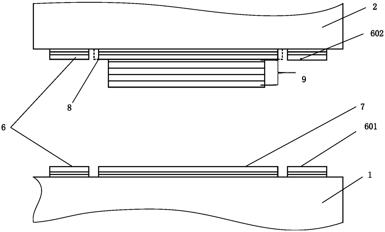
[0046]Step 1, one side of the silicon wafer supporting shell 2 is first made a scribe line by photolithography and etching; the other side of the silicon wafer supporting shell 2 is made a 100 μm deep cavity by photolithography and etching;
[0047] Step 2, vapor-depositing the second anti-reflection film 4 and the getter film 3 on the bottom of the deep cavity;
[0048] Step 3, evaporate the second solder ring 8, the second anti-overflow bar 602 and the third solder ring 9 on the step of the deep cavity;
[0049] Step 4, making a scribe line on the backside of the silicon wafer of the chip 1 by photolithography and etching; evaporating the first solder ring 7 and the first anti-overflow strip 601 on the front side of the silicon wafer of the chip 1;
[0050] Step 5, vacuumize the silicon wafer supporting the shell 2 and the silicon wafer of the chip 1 in the bonding m...
PUM
 Abstract
Description
Claims
Application Information