Wafer-level LED device and preparation method therefor

A LED device, wafer-level technology, applied in semiconductor devices, electrical components, circuits, etc., can solve the problems of low lens aspect ratio, inability to control lens shape, low light efficiency, etc., to improve light efficiency and reduce production. Cost, simple process effect

Pending Publication Date: 2016-06-01
XIAMEN UNIV OF TECH
View PDF4 Cites 0 Cited by
  • Summary
  • Abstract
  • Description
  • Claims
  • Application Information

AI Technical Summary

Problems solved by technology

But the disadvantage of this method is that the shape of the lens depends entirely on the surface tension of the plastic encapsulant, so it is impossible to directly control the shape of the lens, and the aspect ratio of the lens is generally low (that is, the lens is relatively "flat"), and the light effect is relatively low. Low

Method used


Image

  • Wafer-level LED device and preparation method therefor
  • Wafer-level LED device and preparation method therefor
  • Wafer-level LED device and preparation method therefor

Examples


Embodiment Construction

[0027] The present invention will be further described in detail below in conjunction with the accompanying drawings and embodiments. It should be understood that the specific embodiments described here are only used to explain the present invention, but not to limit the present invention. In addition, it should be noted that, for the convenience of description, only some structures related to the present invention are shown in the drawings but not all structures.

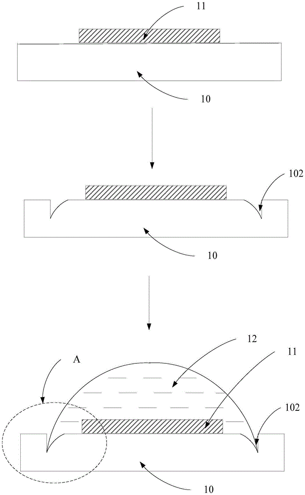
[0028] Please refer to figure 1 , a method for preparing a wafer-level LED device, comprising the following steps:

[0029] S1, providing an LED preform, including a substrate 10 and an LED chip 11 mounted on the substrate 10;

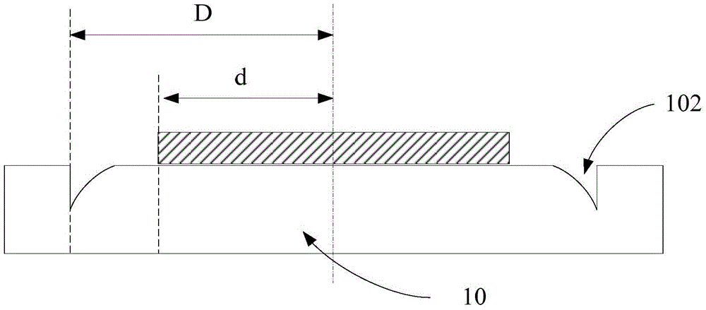
[0030] S2, forming a limiting groove 102 on the substrate 10, the limiting groove 102 surrounds the LED chip 11, and the depth of the limiting groove 102 gradually deepens along a direction away from the LED chip 11;

[0031] S3 , dispensing glue above the LED chip 11 , making the dispen...


PUM


Abstract

The invention discloses a preparation method for a wafer-level LED device. The preparation method comprises the steps of providing an LED prefabricated member, wherein the LED prefabricated member comprises a substrate and an LED chip mounted on the substrate; forming a limiting groove in the substrate, wherein the limiting groove surrounds the LED chip; the depth of the limiting groove is gradually increased in a direction far from the LED chip; performing adhesive dispensing above the LED chip to enable the LED chip to be covered with the dispensed adhesive and to enable the dispensed adhesive to extend to the limiting groove, and then cooling to room temperature to enable the dispensed adhesive to be cured to form a packaging lens layer. The invention also relates to the wafer-level LED device obtained by the preparation method.

Description

technical field [0001] The invention relates to the technical field of LED packaging, in particular to a wafer-level LED device and a preparation method thereof. Background technique [0002] Due to the characteristics of small size, power saving and long life, LED lamps have been increasingly used in lighting, backlighting and other fields. [0003] However, due to the high cost of LED lamps, its further promotion is hindered. Wafer-level LED packaging is an effective way to reduce costs. Wafer-level chip packaging technology is a technology that obtains individual finished chips by packaging and testing the entire wafer and then cutting it. Wafer-level chip-scale packaging technology has changed traditional packages such as ceramic leadless chip carriers, organic leadless chip carriers and digital camera module models, and complied with the market's increasingly light, thin, short, small and low-cost microelectronics products. The requirement of globalization is the cur...

Claims


Application Information

Patent Timeline
Patent Type & Authority Applications(China)
IPC IPC(8): H01L33/54H01L33/58
CPCH01L33/005H01L33/54H01L33/58
Inventor 张旻澍谢安陈文哲林文倩
Owner XIAMEN UNIV OF TECH
Why Eureka
Try Eureka