
Non-isolating switching power supply with high efficiency and high current regulation ratio
A technology of switching power supply and switching power supply circuit, which is applied in the direction of high-efficiency power electronic conversion, conversion of AC power input to DC power output, electrical components, etc., which can solve problems such as unsatisfactory, low power factor and output current adjustment rate, and achieve cost reduction. Effects of reduction, calorific value reduction, and volume reduction
- Summary
- Abstract
- Description
- Claims
- Application Information
AI Technical Summary
Problems solved by technology
Method used
Image

Examples
Embodiment 1
[0024] Example 1: A new high-efficiency high-current regulation non-isolated switching power supply
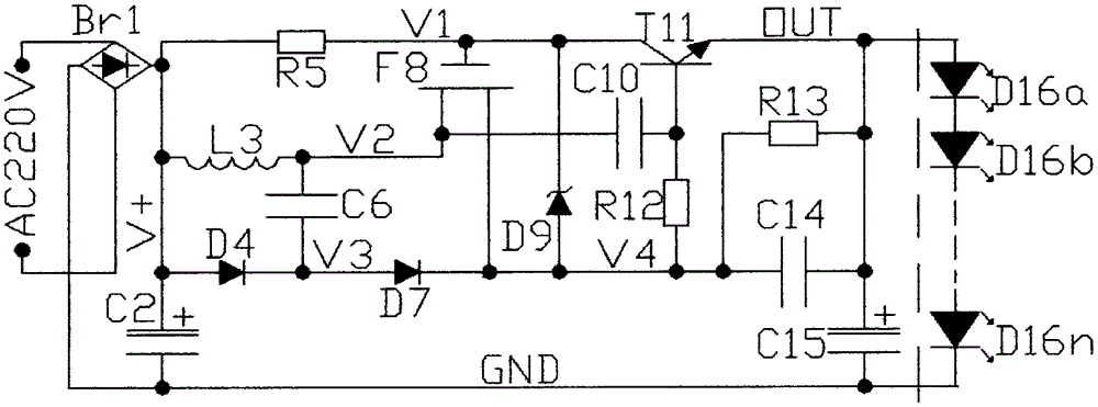
[0025] Such as figure 1 Shown: a non-isolated switching power supply with high efficiency and high current adjustment rate, including rectification and filtering circuit, switching power supply circuit, inductive energy storage recovery circuit and output constant current circuit; where:
[0026] In the rectification circuit composed of rectifier bridge stacks, the input terminals of the rectifier bridge stack Br1 are connected to 220 volts AC mains, and one end of its output is grounded and the other end outputs voltage V+. Between the output voltage line V+ and the ground line A filter capacitor C2 is indirectly installed to form the rectification filter circuit;
[0027]The switching power supply circuit is composed of an inductor L3, a resistor R5, a field effect transistor F8, a Zener diode D9, a capacitor C10, a transistor T11, a resistor R12, a resistor R13, and a capa...
Embodiment 2
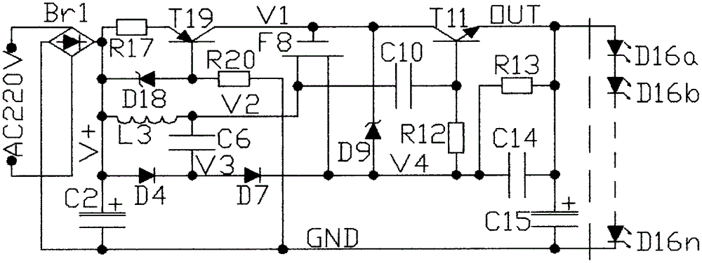
[0033] Embodiment 2: Non-isolated switching power supply with high efficiency and high current regulation rate with constant current source as the load of FET gate electrode circuit
[0034] Such as figure 2 As shown, replace the load resistor R5 in the gate circuit of the field effect transistor F8 with a constant current source composed of a resistor R17, a Zener diode D18, a transistor T19 and a resistor R20, where the collector of the transistor T19 is connected to the V1 voltage line, Its emitter is connected to the output voltage line V+ of the rectifier circuit through a resistor R17, one of its bases is grounded to GND through a resistor R20, and the other base is connected to the output voltage line V+ of the rectifier circuit through a Zener diode D17, so that It can improve the adjustment rate of the output current of the power supply.
[0035] The circuit of this embodiment is relatively complicated, but the current adjustment rate is very high, which can reach 5...
Embodiment 3
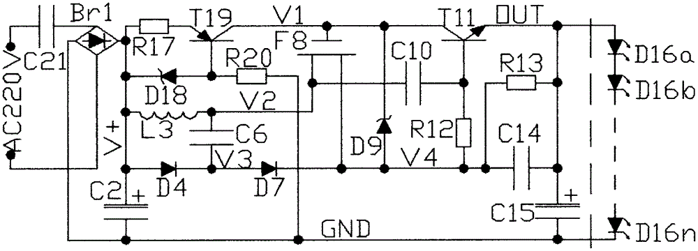
[0036] Embodiment 3: A non-isolated switching power supply with high efficiency and high current adjustment rate with a capacitor on the input arm of the rectifier bridge stack
[0037] Such as image 3 As shown, the resistor R5 connected to the gate of the field effect transistor F8 and the output voltage line V+ is replaced by a constant current source composed of a resistor R17, a Zener diode D18, a transistor T19 and a resistor R20, and an input of the bridge stack Br1 A capacitor C21 that reduces the input voltage of the bridge stack is connected in series between the arm and the 220 volt mains. The circuit in this embodiment is the most complicated. Not only is the current adjustment rate very high, it can reach 5 / 100,000 per volt, and the output voltage can be easily reduced. To a very low level, even the output short circuit will not damage the circuit, it is very practical for occasions with high technical requirements or low voltage power supply.
PUM
 Abstract
Description
Claims
Application Information