Method, device and touch screen device for locating candidate touch points
A touch point and equipment technology, applied in the input/output process of data processing, instruments, electrical digital data processing, etc., can solve the problem of touch point omission
- Summary
- Abstract
- Description
- Claims
- Application Information
AI Technical Summary
Problems solved by technology
Method used
Image
Examples
Embodiment 1
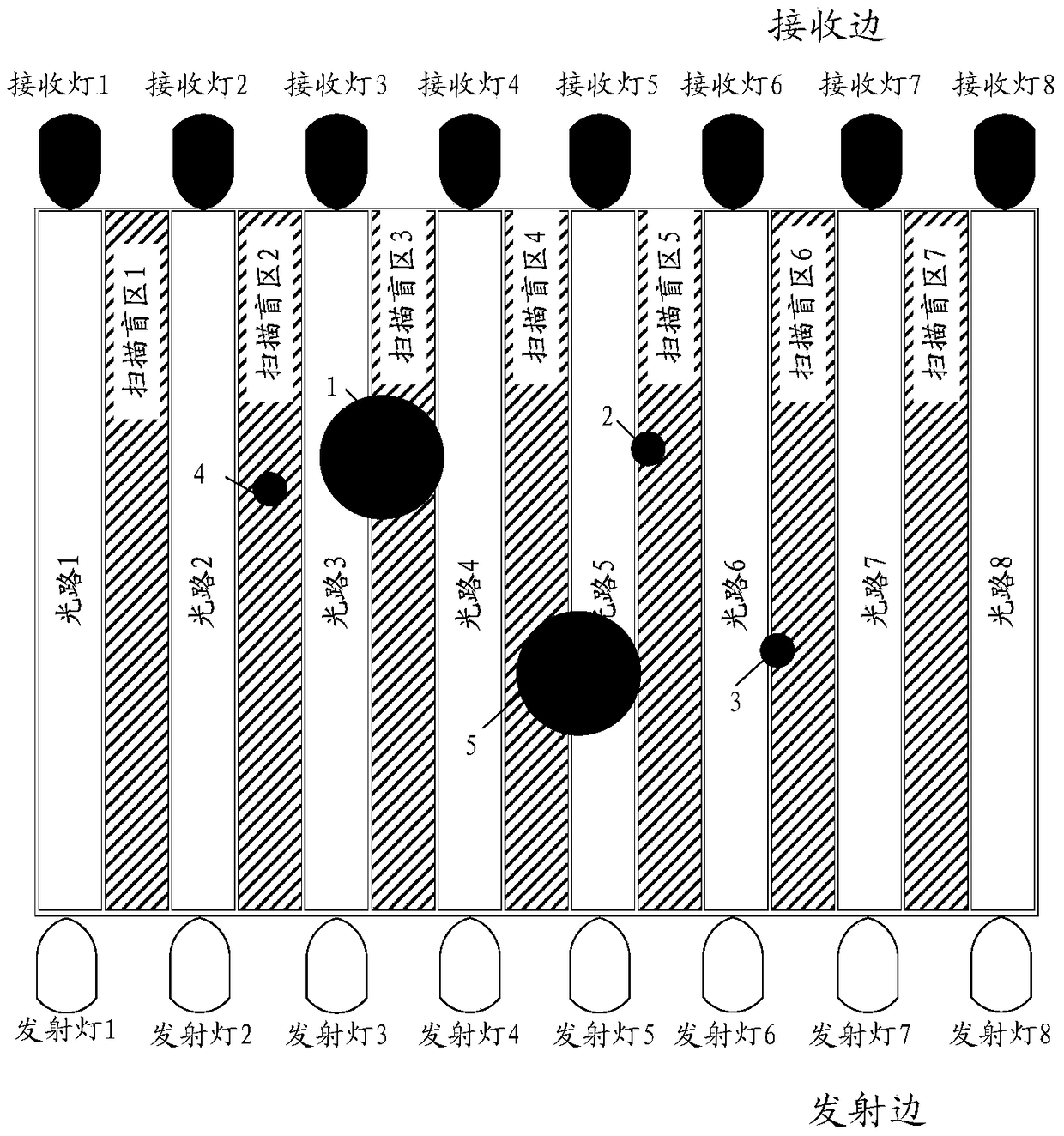
[0060] Embodiments of the present invention provide a method for locating candidate touch points, which is applied to touch screen devices, such as Figure 5 As shown, the method for positioning candidate touch points includes:
[0061] S101. The device for locating candidate touch points acquires the optical path voltage values on each optical path in the first scanning direction and the optical path voltage values on each optical path in the second scanning direction within one scanning period.
[0062] Wherein, the optical path voltage value on each optical path in the first scanning direction corresponds to the voltage value corresponding to the optical signal received by the receiving lamp corresponding to each optical path in the first scanning direction. The optical path voltage value on each optical path in the second scanning direction corresponds to the voltage value corresponding to the optical signal received by the receiving lamp corresponding to each optical ...
Embodiment 2
[0151] An embodiment of the present invention provides a device for locating candidate touch points, which is included in a touch screen device, such as Figure 25 As shown, the device for locating candidate touch points includes: an acquisition module 21 , an assignment module 22 , a determination module 23 and a calculation module 24 .
[0152] The acquiring module 21 is configured to acquire the optical path voltage values on each optical path in the first scanning direction and the optical path voltage values on each optical path in the second scanning direction within one scanning period, and the optical path voltage values on each optical path are set by The voltage values corresponding to the optical signals received by the receiving lamps corresponding to the above-mentioned respective optical paths.
[0153] An assignment module 22, assigning the optical path voltage values of each blind scanning area in the first scanning direction and the optical path volt...
PUM
 Abstract
Description
Claims
Application Information


