

Fingerprint identification apparatus, manufacturing method for fingerprint identification apparatus, array substrate and display apparatus
A technology for fingerprint identification and array substrate, which is used in character and pattern identification, acquisition/organization of fingerprints/palmprints, detection of live fingers, etc., and can solve the problem of large thickness of fingerprint identification devices.
- Summary
- Abstract
- Description
- Claims
- Application Information
AI Technical Summary
Problems solved by technology
Method used
Image

Examples
Embodiment 1
[0075] In this embodiment, the above-mentioned fingerprint recognition device is disposed in the above-mentioned display area 40 .
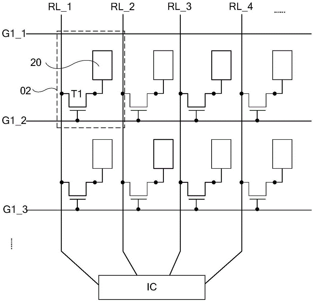
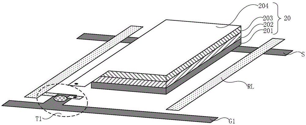
[0076] For example, it can be found in Figure 6 As shown in each sub-pixel 01, set a figure 2 Fingerprint recognition unit 02 is shown. Specifically, such as Figure 7 As shown, the first transistor T1 and the photosensitive device 20 in the fingerprint identification unit 02 are arranged in one sub-pixel 01 .
[0077] In this way, fingerprint identification can be realized in the display area 40 .
[0078] In addition, since the second gate line G2 and the data line D can cross to define the sub-pixel 01 , and the first gate line G1 and the reading signal line RL can define the fingerprint identification unit 02 . Therefore, in order to make the wiring structure on the entire array substrate neat, preferably, the first gate line G1 can be parallel to the second gate line G2, and the read signal line RL can be parallel to the data line D. ...
Embodiment 2
[0080] In this embodiment, the above-mentioned fingerprint recognition device is also arranged in the display area 40 . The difference from the first embodiment is that not every sub-pixel 01 in this embodiment is provided with the above-mentioned fingerprint recognition unit 02 .
[0081] Specifically, the above-mentioned fingerprint identification unit 02 may be set in a sub-pixel in the reconfigured pixel unit. For example, when the sub-pixels constituting the pixel unit include the first color sub-pixel 110, the second color sub-pixel 111, and the third color sub-pixel 112, the fingerprint recognition unit 02 can be arranged on the first color sub-pixel 110, the second color sub-pixel In the sub-pixel 111 or the sub-pixel 112 of the third color. Wherein, the above-mentioned first color, second color and third color constitute three primary colors.
[0082] Alternatively, when the display area 40 includes pixel units such as Figure 8 As shown, when the first color sub-pi...
PUM
| Property | Measurement | Unit |
|---|---|---|
| Thickness | aaaaa | aaaaa |
| Thickness | aaaaa | aaaaa |
| Thickness | aaaaa | aaaaa |
Abstract
Description
Claims
Application Information