Touch panel and preparation method thereof

A technology of a touch panel and a manufacturing method, which are applied in the directions of instruments, electrical digital data processing, and data processing input/output processes, etc., can solve the problems of the complex structure of the capacitive touch screen film layer, reduce the manufacturing cost, etc. The effect of manufacturing cost, improving overall strength, and simplifying film structure

Pending Publication Date: 2016-05-11
SHENZHEN LAIBAO HI TECH +1
View PDF3 Cites 3 Cited by
  • Summary
  • Abstract
  • Description
  • Claims
  • Application Information

AI Technical Summary

Problems solved by technology

Therefore, the film structure of the capacitive touch screen is complicated, which is not conducive to reducing the production cost.

Method used


Image

  • Touch panel and preparation method thereof
  • Touch panel and preparation method thereof
  • Touch panel and preparation method thereof

Examples


Embodiment Construction

[0021] In order to illustrate the touch panel provided by the present invention and the manufacturing method thereof, a detailed description will be given below in conjunction with the accompanying drawings and text descriptions of the specification.

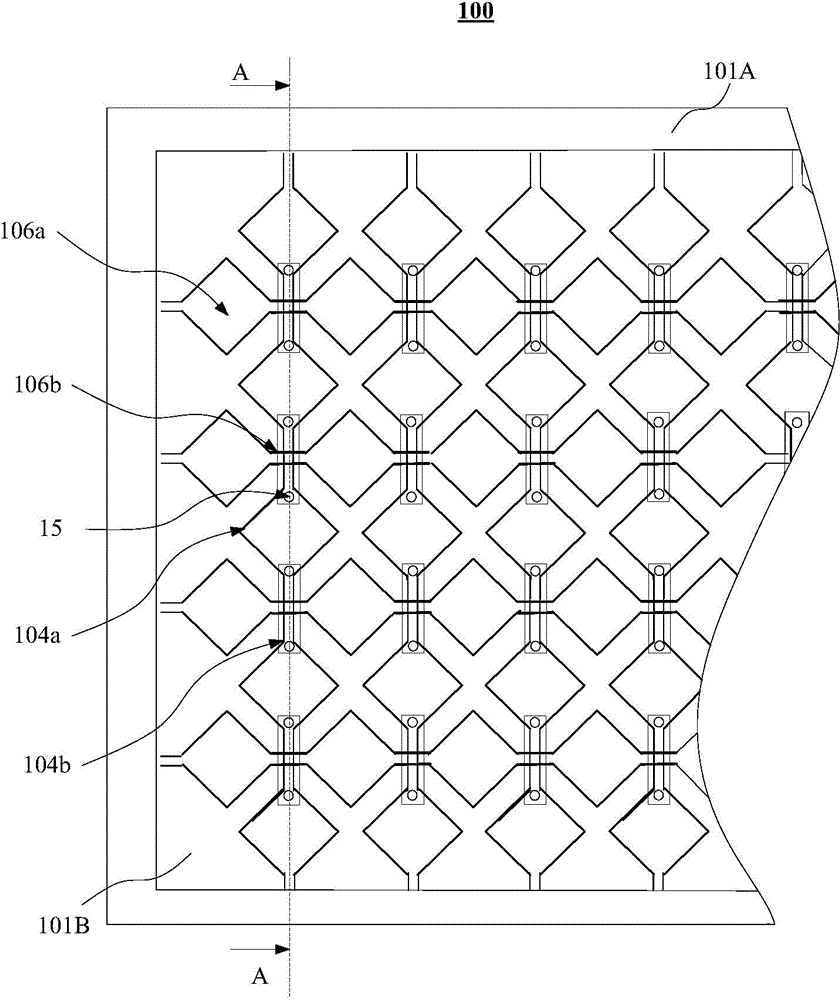
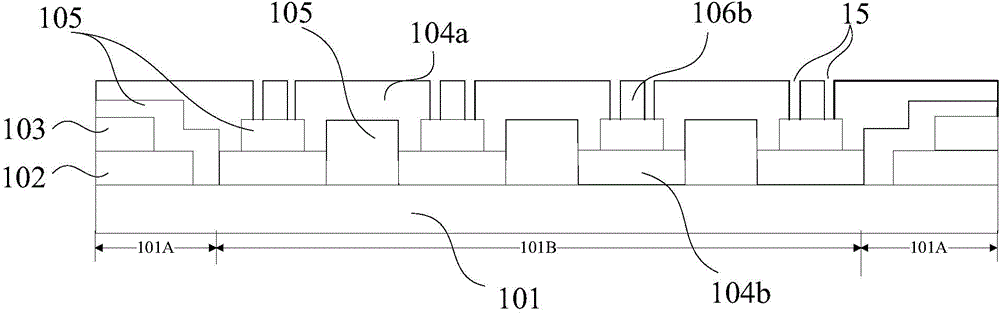
[0022] Please refer to figure 1 , figure 2 , which is a schematic structural diagram of a touch panel 100 according to a preferred embodiment of the present invention and a schematic structural diagram of the touch panel 100 along the direction A-A. The touch panel 100 at least includes a substrate 101 , a shielding layer 102 , a conductive lead layer 103 and a touch layer.

[0023] The substrate 101 has at least a first surface 101a, and the first surface 101a is a plane. In other embodiments, the first surface may also be a curved surface or an irregular surface. The substrate 101 is made of transparent materials such as glass and resin. The first surface 101a includes at least a first region 101A and a second region 101B....


PUM


Abstract

The invention relates to a panel display technical field, especially a touch panel. The touch panel at least comprises a base plate; the base plate at least is equipped with a first surface; the first surface at least comprises a first area and a second area; the second area is located at least at one side of the first area; the touch panel also comprises a conductive lead wire layer which is formed on the first surface on which the second area is located, and a touch layer which is formed on the first surface on which the first area is located; the touch layer and the conductive lead wire layer are electrically connected; the touch layer at least comprises an insulation layer; and the insulation layer covers the first surface on which the conductive lead wire layer and the first area are located. Moreover, the invention discloses a preparation method of the panel display.

Description

technical field [0001] The invention relates to the field of flat panel display technology, in particular to a touch panel and a manufacturing method thereof. Background technique [0002] The manufacturing method of the existing capacitive touch screen is usually: first make the touch electrode in the touch area of ​​a glass substrate; The touch electrodes lead to the processor. However, in order to prevent the conductive lead layer in the capacitive touch screen with the above structure from being affected by the external environment, it is usually necessary to form another protective layer on the conductive lead layer. Therefore, the film layer structure of the manufactured capacitive touch screen is complicated, which is not conducive to reducing the manufacturing cost. Contents of the invention [0003] In view of this, the present invention provides a touch panel with a simple film structure, which is beneficial to reduce manufacturing costs. [0004] In addition,...

Claims


Application Information

Patent Timeline
Patent Type & Authority Applications(China)
IPC IPC(8): G06F3/044
Inventor 王士敏汪征朱泽力张超李绍宗
Owner SHENZHEN LAIBAO HI TECH
Why Eureka
Try Eureka