
Highly-efficient interconnected system capable of configuring chips and realization system thereof and device

An interconnected system and high-efficiency technology, applied in the field of system-on-chip, can solve problems such as adverse power consumption and cost control, increased bus protocol overhead, design and verification impact, etc., to save design time, reduce power consumption, and optimize delays. Effect

Active Publication Date: 2016-06-15
SANECHIPS TECH CO LTD
View PDF4 Cites 6 Cited by
  • Summary
  • Abstract
  • Description
  • Claims
  • Application Information

AI Technical Summary

Problems solved by technology

[0005] However, the bit width of the ID increases with the increase of the interconnection depth, resulting in an increase in the bus protocol overhead, high power consumption, and high cost expenditure; secondly, ID conversion (ID conversion by the adapter) can be used to achieve different ID widths. Bus interconnection increases access delay, affects design, verification, back-end implementation, etc., and is not conducive to power consumption and cost control

Method used


Image

  • Highly-efficient interconnected system capable of configuring chips and realization system thereof and device
  • Highly-efficient interconnected system capable of configuring chips and realization system thereof and device
  • Highly-efficient interconnected system capable of configuring chips and realization system thereof and device

Examples


Embodiment Construction

[0034] For the convenience of description, the existing interconnection system adopting ID bit width incremental mode and its communication method are described below.

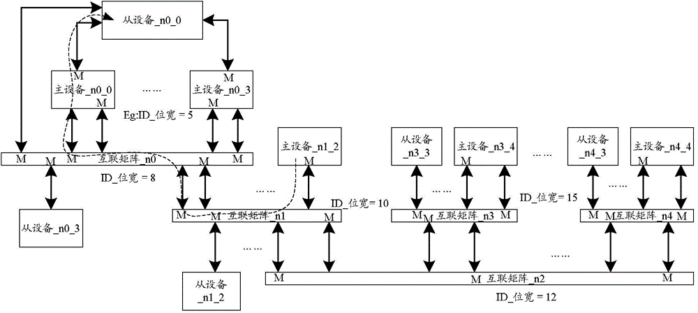
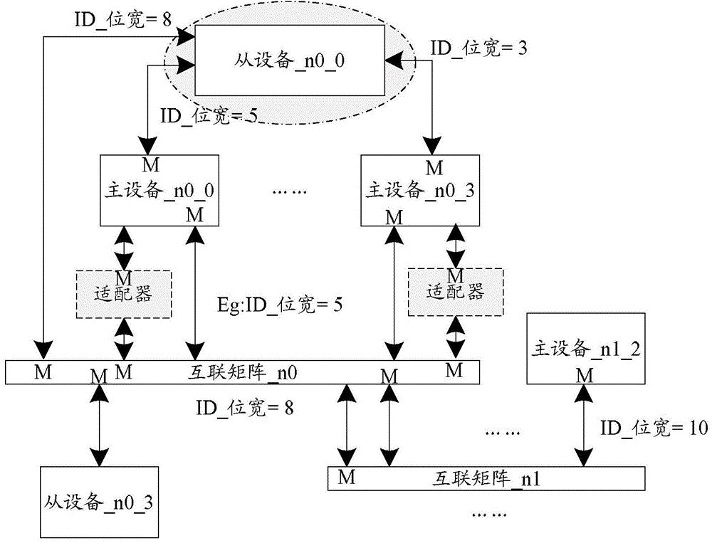
[0035] Here, the devices connected to the bus (not limited to devices, may also be subsystems) are referred to as components. figure 1 The M shown in the figure represents the master device interface, and the other end of the double-headed arrow represents the slave device interface; some components on the system have only the master device interface, some have only the slave device interface, and some have both master and slave device interfaces. The master device interface for accessing the master device_n0_0 does not need to be interconnected through the Matrix or the Crossbar, therefore, the master device_n0_0 is not included in the scope of interconnected master devices.

[0036] figure 1 Among all the master device interfaces above, it is assumed that the master device _n0_0 has the most different reque...


PUM


Abstract

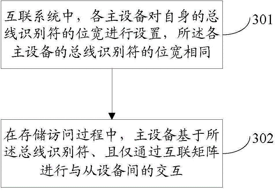
The invention discloses a highly-efficient interconnected system capable of configuring chips. The method comprises following steps: setting the bit widths of bus identifiers of all main equipment in the interconnected system, wherein bit widths of bus identifiers of all main equipment are the same; and interacting the main equipment with secondary equipment via an interconnected matrix during storage and access processes based on the bus identifiers. Meanwhile, the invention further discloses a realization system achieving the method and a device.

Description

technical field [0001] The invention relates to a system-on-chip (SOC) in the communication field, in particular to an efficient configurable on-chip interconnection system and its realization method and device. Background technique [0002] With the continuous improvement of the manufacturing process, there are more and more transistors inside the chip, and the on-chip system is becoming more and more complex, usually integrating dozens or even hundreds of IP cores, and inter-core communication has become one of the main problems in SOC design. . For complex systems, the shared interconnection system in the standard is generally selected. [0003] In a complex shared interconnection system, all communication can be transformed into mutual storage access, the party that sends out the storage access request is the master device, and the party that receives the storage access request is the slave device. SOC is a system that connects many master devices and slave devices. ...

Claims


Application Information

Patent Timeline
Patent Type & Authority Applications(China)
IPC IPC(8): G06F13/40
CPCG06F13/4022G06F13/4265Y02D10/00G06F13/38G06F13/1678G06F13/364G06F13/4018G06F13/4282
Inventor 蒋建平
Owner SANECHIPS TECH CO LTD
Learn More