A rfid tag integrated in pcba

A technology of RFID tags and tags, which is applied to record carriers, instruments, and calculations used by machines, can solve the problems of complex manufacturing process, high single cost, and large surface area, and achieve good radiation performance, save surface area, and be easy to integrate Effect

Active Publication Date: 2019-06-11
CHINA JILIANG UNIV
View PDF6 Cites 0 Cited by
  • Summary
  • Abstract
  • Description
  • Claims
  • Application Information

AI Technical Summary

Problems solved by technology

RFID tags are PET-based inlays. This type of inlay is generally in the form of a dipole antenna. Due to its large surface area and complex manufacturing process, the cost of a single tag is high and cannot be widely promoted.
Anti-metal tags based on PCB substrates, such tags are often made into small-volume tag modules, with high single cost, and cannot be integrated into the original circuit structure of PCBA

Method used


Image

  • A rfid tag integrated in pcba
  • A rfid tag integrated in pcba
  • A rfid tag integrated in pcba

Examples


Embodiment Construction

[0020] The present invention will be described in further detail below in conjunction with the accompanying drawings and specific embodiments.

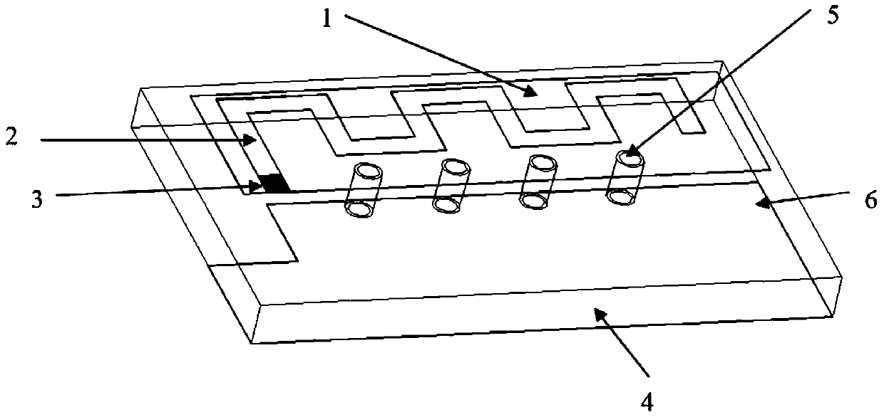
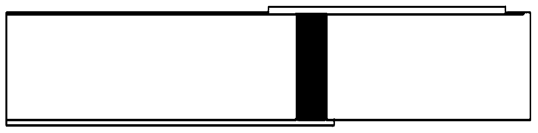
[0021] Such as Figure 1-4 As shown, a kind of RFID label integrated in PCBA provided by the present invention, this label is integrated in the edge of PCBA, is made of label antenna and label chip 3; It is a part of the PCB copper-clad wiring. The upper radiation surface is the top layer of the circuit board, which is used as the main radiation surface 1 of the tag antenna, and the lower radiation surface is the bottom layer of the circuit board, which is used as the ground plane 6 of the tag antenna. A common substrate 4 for PCBA; the substrate 4 can be selected from polyimide or glass fiber epoxy resin.

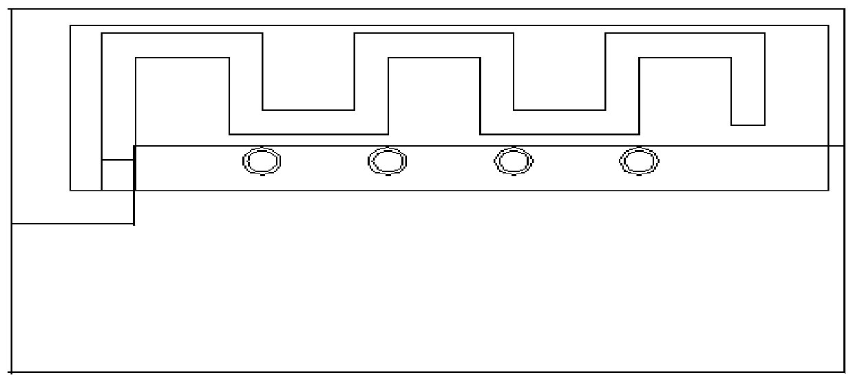
[0022] Such as figure 2 As shown, the main radiation surface 1 of the label is a tooth-shaped gap structure 2, and the feeder part of the tag chip 3 is located at the initial position of the tooth-shaped gap; the tooth-shaped g...


PUM


Abstract

The invention discloses an RFID label integrated on a PCBA. The label is located on the edge of a general multi-layer circuit board. The label is composed of a label antenna and a label chip. The label antenna is composed of an upper layer of radiation surface and a lower layer of radiation surface. The radiation surfaces of the label antenna form one part of PCB copper coating wiring; the upper layer of radiation surface is the top layer of the circuit board and is taken as the master radiation surface of the label antenna; the lower layer of radiation surface is the bottom layer of the circuit board and is taken as the grounding surface of the label antenna; the middle part of the upper layer and lower layer is a substrate shared with the PCBA; the master radiation surface of the label is a tooth-shaped slot structure; and the feed part of the label chip is located at the starting position of a tooth-shaped slot. According to the label, the grounding surface of the circuit board and the upper layer of master radiation body form a slot antenna; the general RFID label chip is directly adhered at the feed port; with respect to the general double-layer circuit board, the surface area of the PCBA is saved; it is unnecessary to adhere the extra RFID label; the RFID label is formed on the surface of the PCBA only by one RFID chip; and compared with other information traceback carrier, the label has the advantages of small area and low cost.

Description

technical field [0001] The invention relates to the technical field of RFID, in particular to an RFID tag integrated in a PCBA. Background technique [0002] At present, RFID technology has been applied in security protection, supply chain management, ID card and ticket management, food safety traceability management and other fields, but it has not been applied in the information traceability of the production process of electronic and electrical products and product life cycle management so far. In the case, the key information carrier is the RFID tag integrated in the product PCBA. [0003] The RFID system is mainly composed of four parts: electronic tags, readers, reader antennas, and middleware. The reader sends a radio frequency signal of a certain frequency through the transmitting antenna. When the electronic tag enters the working area of ​​the transmitting antenna, an induced current is generated, and the electronic tag obtains energy and is activated; the electro...

Claims


Application Information

Patent Timeline
Patent Type & Authority Patents(China)
IPC IPC(8): G06K19/077
CPCG06K19/0772G06K19/07749
Inventor 洪涛蒋天齐张松顾素敏熊戈武萌
Owner CHINA JILIANG UNIV
Why Eureka
Try Eureka