Low-damage buried mercury cadmium telluride detector chip

A detector chip, mercury cadmium telluride technology, applied in semiconductor devices, electrical components, circuits, etc., can solve problems such as blind elements and detector performance degradation

Active Publication Date: 2016-07-13
SHANGHAI INST OF TECHNICAL PHYSICS - CHINESE ACAD OF SCI
View PDF5 Cites 4 Cited by
  • Summary
  • Abstract
  • Description
  • Claims
  • Application Information

AI Technical Summary

Problems solved by technology

Traditional HgCdTe devices mostly adopt a planar device structure, that is, the n-type and p-type regions of the photosensitive element are located on the surface of the material. Regions cause defects to increase in value and cause detector performance to degrade, and even cause blind elements

Method used


Image

  • Low-damage buried mercury cadmium telluride detector chip

Examples


Embodiment Construction

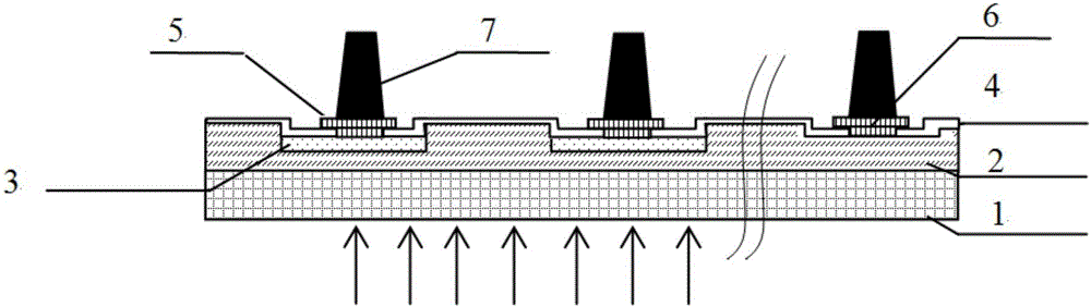
[0009] The specific implementation of this patent will be described in detail below by taking a 640×512 Si-based medium-wave mercury cadmium telluride focal plane chip with a pixel center distance of 25 μm as an example in conjunction with the accompanying drawings:

[0010] The epitaxial material for preparing the low-damage buried junction HgCdTe detector chip is a p-type Hg vacancy-doped Si-based HgCdTe film material prepared by molecular beam epitaxy, the material composition x = 0.3, and the thickness of the HgCdTe layer is is 5 μm.

[0011] Such as figure 1 As shown, the low-damage buried junction mercury cadmium telluride detector chip of the present invention includes: a substrate 101, a mercury cadmium telluride p-type epitaxial film 2, a photosensitive element n-type region 3, a passivation layer 4, and an n-type region electrode 7, P-type region electrode 5, indium column array 6. The photosensitive element n-type region array 3 is formed by boron ion implantation...


PUM


Abstract

The invention discloses a low-damage buried mercury cadmium telluride detector chip, the chip comprises a substrate, a mercury cadmium telluride p-type epitaxial thin film, an ion implantation n-type region, a passivation layer, an n-type region electrode, a p-type electrode and an indium bump array, and the invention relates to the technology of photoelectric detector. According to the invention, a structure scheme of p-n node being prepared in a mercury cadmium telluride material etch pit is adopted, so that the position of the node region is far away from the material surface, problems including detector performance reduction, blind pixels increasing and the like caused by defects increasing caused by the acting force of a photosensitive element region form technologies such as cleaning, adhesive removing and the like are avoided. The chip has a great help to reduce blind pixel ratio of a mercury cadmium telluride plane.

Description

technical field [0001] The patent of the present invention relates to a mercury cadmium telluride infrared detector, specifically a low-damage buried junction mercury cadmium telluride infrared detector chip. Background technique [0002] Mercury cadmium telluride material is an ideal infrared detector material, which has the advantages of adjustable band gap, high internal quantum efficiency, and high mobility of electrons and holes. With the maturity of molecular beam epitaxy preparation technology for Si-based HgCdTe materials, the limitation of material size has been broken through, the cost of material preparation has been reduced, and the yield rate has been increased. The third generation of HgCdTe detectors is developing towards the direction of large area array, multicolor, miniaturization and low cost. However, with the expansion of the area array scale and the decrease of the pixel center distance, the blind element problem becomes a key problem restricting the p...

Claims


Application Information

Patent Timeline
Patent Type & Authority Applications(China)
IPC IPC(8): H01L31/0352H01L31/103
CPCH01L31/03529H01L31/1032
Inventor 胡晓宁张姗樊华廖清君叶振华林春丁瑞军何力
Owner SHANGHAI INST OF TECHNICAL PHYSICS - CHINESE ACAD OF SCI
Why Eureka
Try Eureka