Method and device for position calibration

A calibration plate and coordinate technology, applied in the field of film loading technology and optics, can solve the problems such as the inability to eliminate small deviations and the difficulty in improving the precision of film loading, achieve simple and accurate verification and correction of deviations, eliminate small deviations, and improve the accuracy of equipment Effect

Active Publication Date: 2018-09-11
CETC BEIJING ELECTRONICS EQUIP
View PDF7 Cites 0 Cited by
  • Summary
  • Abstract
  • Description
  • Claims
  • Application Information

AI Technical Summary

Problems solved by technology

At present, in the chip loading equipment, the chip is usually loaded directly after picking up the chip, but there is a major problem in this method. After picking up the chip, it is directly loaded without alignment, so it is impossible to eliminate the slight deviation that may exist during picking, making the chip loading difficult. It is difficult to improve the accuracy of

Method used


Image

  • Method and device for position calibration
  • Method and device for position calibration
  • Method and device for position calibration

Examples


Embodiment Construction

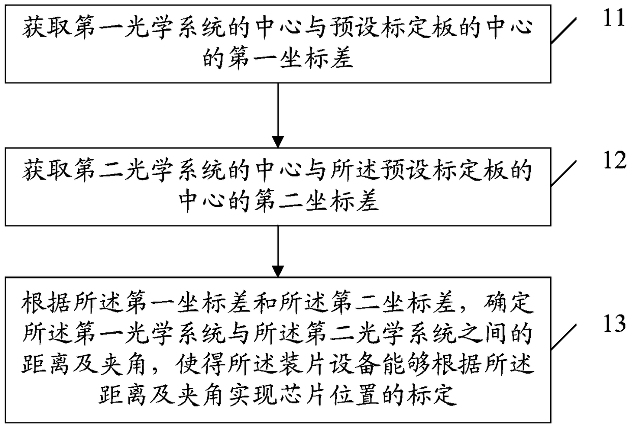
[0051] In order to make the technical problems, technical solutions and advantages to be solved by the present invention clearer, the following will describe in detail with reference to the drawings and specific embodiments.

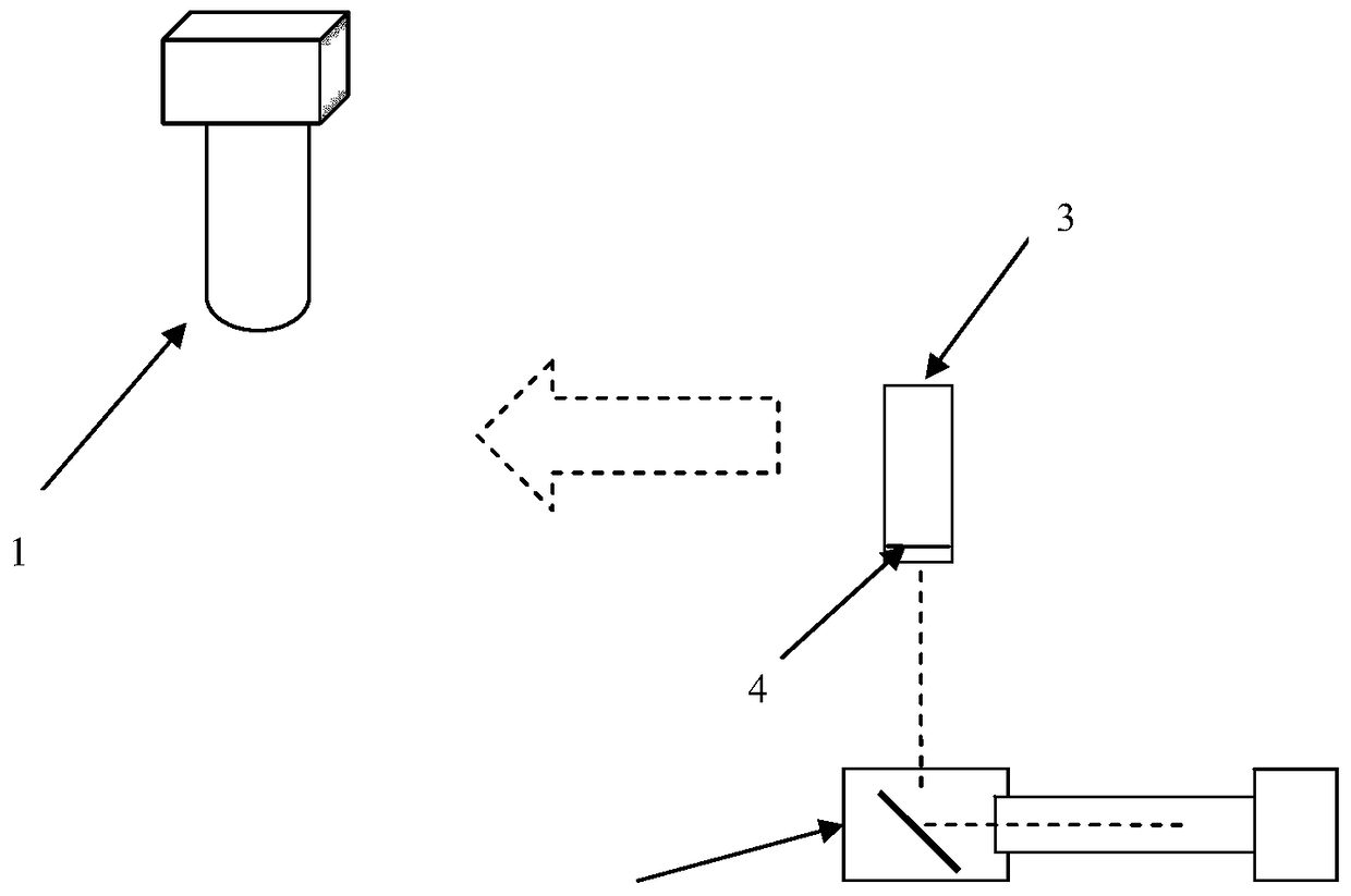
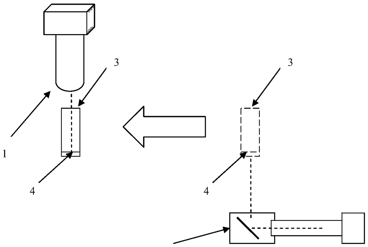
[0052]The present invention aims at the problem in the prior art that the chips picked up by the chip loading equipment are loaded directly without alignment, and there is a slight deviation, which makes the chip loading precision not high. Previously, the precise distance and angle between the first optical system and the second optical system were determined through the first coordinate difference and the second coordinate difference, so that the loading equipment can realize the calibration of the chip position according to the distance and the angle, eliminating the The slight deviation that may occur during the chip picking process meets higher chip loading accuracy requirements; at the same time, it solves the problem of inconsistent coordinate syst...


PUM


Abstract

The invention provides a position calibrating method and a position calibrating device, which are disposed in a chip mounting device. The position calibrating method is characterized in that a first coordinate difference between a center of a first optical system and a center of a preset calibrating plate can be acquired, and the preset calibrating plate can be moved to the visual field of the first optical system according to the preset technological track; a second coordinate difference between a center of a second optical system and the center of the preset calibrating plate can be acquired, and the preset calibrating plate can be moved from the visual field of the first optical system to the visual field of the second optical system according to the preset technological track; the distance and the included angle between the first optical system and the second optical system can be determined according to the first coordinate difference and the second coordinate difference, and then the chip mounting device can be used for the calibrating of the chip position according to the distance and the included angle. The calibrated distance and the calibrated included angle between the optical systems can be used to guarantee the precision of the chip mounting technology of the next step, and therefore the high precision chip mounting can be realized.

Description

technical field [0001] The invention relates to the fields of film loading technology and optical technology, in particular to a method and device for position calibration. Background technique [0002] With the rapid development of global electronic information technology, integrated circuit chips continue to develop in the direction of high density, high performance, thinness and shortness. In order to meet the requirements of IC packaging, the number of bumps on the chip will increase. With the increase in the number of bumps, it poses challenges to the existing chip mounting equipment. One of the main problems is how to mount chips with high density and small pitch bumps with high precision. At present, in the chip loading equipment, the chip is generally loaded directly after picking up the chip, but there is a major problem in this method. After picking up the chip, it is directly loaded without alignment, so it is impossible to eliminate the slight deviation that may ...

Claims


Application Information

Patent Timeline
Patent Type & Authority Patents(China)
IPC IPC(8): G01B11/00G01B11/14G01B11/26
Inventor 李恺霍杰刘子阳李向东叶乐志唐亮
Owner CETC BEIJING ELECTRONICS EQUIP
Why Eureka
Try Eureka