Pre-alignment system and method for bonding flip chip

A flip-chip and pre-alignment technology, which is applied in the manufacture of electrical components, electrical solid devices, semiconductor/solid devices, etc., can solve the problems of difficulty in improving chip loading accuracy and inability to eliminate small deviations, so as to improve accuracy and efficiency, The effect of accurately correcting deviations and eliminating small deviations

Active Publication Date: 2015-10-28
CETC BEIJING ELECTRONICS EQUIP
View PDF4 Cites 8 Cited by
  • Summary
  • Abstract
  • Description
  • Claims
  • Application Information

AI Technical Summary

Problems solved by technology

[0003] At present, in the chip loading equipment, the chips are generally picked up and dipped in glue to complete the chip loading directly. However, there is a major problem in this method: after picking up the chips, they are directly loaded without pre-alignment, so it is impossible to eliminate the slight deviation that may exist during picking. It is difficult to improve the accuracy of film loading

Method used


Image

  • Pre-alignment system and method for bonding flip chip
  • Pre-alignment system and method for bonding flip chip
  • Pre-alignment system and method for bonding flip chip

Examples


Embodiment 1

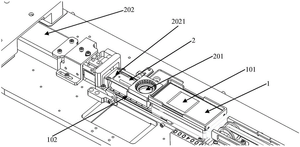
[0038] According to one aspect of the present invention, a pre-alignment system for flip-chip bonding is provided, such as figure 1 As shown, the pre-alignment system includes:

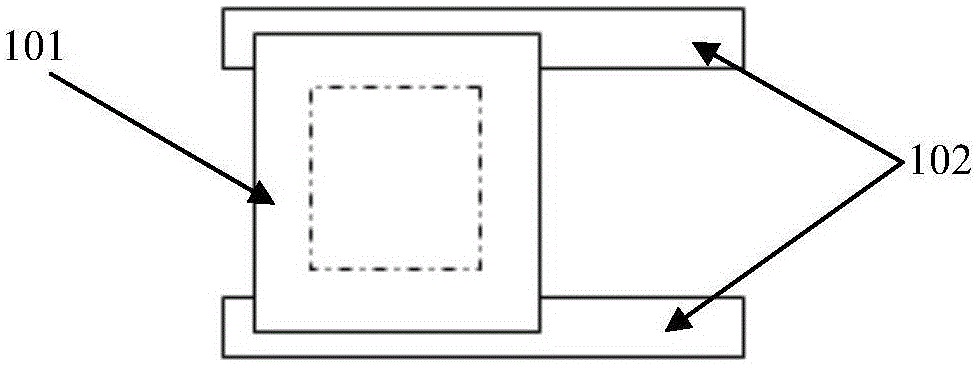
[0039] The flip-chip dipping structure 1 installed on the workbench, the flip-chip dipping structure 1 includes: a dipping plate 101 for flip-chip dipping; mechanical slide rails slidingly connected to both sides of the dipping plate 101 102; a motor electrically connected to the mechanical slide rail 102 and used to drive the mechanical slide rail 102 to slide;

[0040] The up-view optical structure 2 installed on the workbench, the up-view optical structure 2 includes: a turning prism 201 fixed between the mechanical slide rails 102 and located below the dipping plate 101; an industrial camera for obtaining flip-chip images 202; Wherein, the turning prism 201 is connected with the industrial camera 202 through the lens 2021 of the industrial camera 202, and

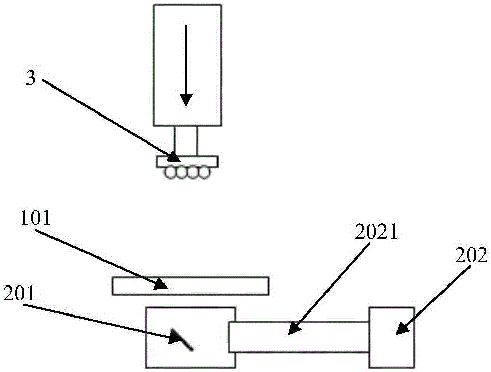
[0041] Such as image 3 As shown in ,...

Embodiment 2

[0050] In an embodiment of the present invention, a pre-alignment method for flip-chip bonding is provided, which is applied to the above-mentioned pre-alignment system for flip-chip bonding. The pre-alignment system includes: Flip-chip dipping structure 1, the flip-chip dipping structure 1 includes: a dipping plate 101 for flip-chip dipping; mechanical slide rails 102 slidingly connected to both sides of the dipping plate 101; 102 is electrically connected, and is used to drive the motor for sliding the mechanical slide rail 102; the upward-looking optical structure 2 installed on the workbench, the upward-looking optical structure 2 includes: fixed between the mechanical slide rails 102, and located below the rubber dipping plate 101 A turning prism 201; an industrial camera 202 for obtaining flip-chip images; wherein, the turning prism 201 and the industrial camera 202 are connected through the lens 2021 of the industrial camera 202, and are located above the glue board 101 ...


PUM


Abstract

The invention provides a pre-alignment system and a pre-alignment method for bonding flip chips. The pre-alignment system comprises a flip chip glue dipping structure, an upper vision optical structure and a flip chip placement head, wherein the flip chip glue dipping structure comprises a glue dipping plate, mechanical sliding rails connected with two sides of the glue dipping plate in a slided manner, and a motor driving the mechanical sliding rails to slide; and the upper vision optical structure comprises a deflecting prism which is fixed between the mechanical sliding rails and arranged under the glue dipping plate, and an industrial camera acquiring images of the flip chips. According to the pre-alignment system and the pre-alignment method, the flip chip placement head picks up one flip chip, moves to a position above the glue dipping plate for dipping glue according to a first trajectory and is lifted upwards after the glue dipping of the flip chip is finished, the mechanical sliding rails drives the glue dipping plate to slide according to a second trajectory and avert from the deflecting prism, then the flip chip after glue dipping is pre-aligned via the upper vision optical structure. Through the pre-alignment system provided by the invention, the bonding accuracy and efficiency are greatly increased, and the requirements of high-precision chip loading are satisfied.

Description

technical field [0001] The invention relates to the technical field of flip-chip bonding, in particular to a pre-alignment system and method for flip-chip bonding. Background technique [0002] With the rapid development of global electronic information technology, integrated circuit chips continue to develop in the direction of high density, high performance, thinness and shortness. In order to meet the packaging requirements of IC (Integrated Circuit, integrated circuit), the number of bumps on the chip will increase. more. With the increase in the number of bumps, it poses challenges to the existing chip mounting equipment. One of the main problems is how to mount chips with high density and small pitch bumps with high precision. [0003] At present, in the chip loading equipment, the chips are generally picked up and dipped in glue to complete the chip loading directly, but there is a major problem in this method: after picking up the chips, they are directly loaded wit...

Claims


Application Information

Patent Timeline
Patent Type & Authority Applications(China)
IPC IPC(8): H01L21/68
CPCH01L21/68H01L2224/80122
Inventor 唐亮李恺叶乐志
Owner CETC BEIJING ELECTRONICS EQUIP
Why Eureka
Try Eureka