Light emitting diode and manufacturing method therefor

A technology of light-emitting diodes and electrodes, which is applied in the direction of electrical components, circuits, semiconductor devices, etc., and can solve problems that affect LED light extraction rate, current waste, waste, etc.

Active Publication Date: 2016-08-10
TIANJIN SANAN OPTOELECTRONICS
View PDF8 Cites 11 Cited by
  • Summary
  • Abstract
  • Description
  • Claims
  • Application Information

AI Technical Summary

Problems solved by technology

Although this structure can meet the high power demand, it itself wastes a lot
Please see figure 2 , in this design, the second wire electrode (wire electrode) is relatively large. After the current is turned on, the current is poured into the active layer below the first wire electrode in a large proportion and emits light compositely. Most of the emitted l

Method used


Image

  • Light emitting diode and manufacturing method therefor
  • Light emitting diode and manufacturing method therefor
  • Light emitting diode and manufacturing method therefor

Examples


Embodiment Construction

[0044] The implementation of the present invention will be described in detail below in conjunction with the accompanying drawings and examples, so as to fully understand and implement the process of how to apply technical means to solve technical problems and achieve technical effects in the present invention. It should be noted that, as long as there is no conflict, each embodiment and each feature in each embodiment of the present invention can be combined with each other, and the formed technical solutions are all within the protection scope of the present invention.

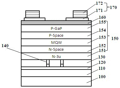
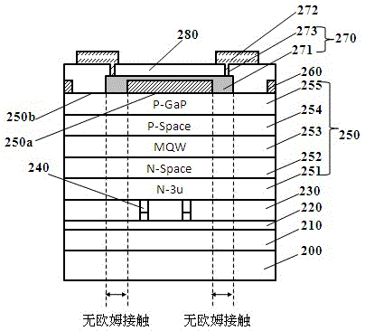
[0045] Please see image 3, a light-emitting diode implemented according to the present invention, including: a conductive substrate 200, a metal bonding layer 210, a conductive reflective layer 220, a transparent dielectric layer 230, a light-emitting epitaxial stack 250, an ohmic contact layer 260, an extended electrode 271, The transparent insulating layer 280 and the wire electrode 272 . Wherein the con...


PUM


Abstract

The invention discloses a light emitting diode and a manufacturing method therefor. The light emitting diode comprises a light emitting epitaxial laminated layer, an ohmic contact layer, an extending electrode, a transparent insulating layer, and a bonding wire electrode, wherein the upper surface of the light emitting epitaxial laminated layer is divided into an ohmic contact region and a non-ohmic contact region; the ohmic contact layer is positioned on the ohmic contact region of the light emitting epitaxial laminated layer; the extending electrode is formed on the ohmic contact layer, and at least partially extends towards the edge of the ohmic contact layer until reaches the non-ohmic contact region of the light emitting epitaxial laminated layer to be in contact with the upper surface of the light emitting epitaxial laminated layer; the extending electrode and the upper surfaces of the exposed ohmic contact layer and the light emitting epitaxial laminated layer are covered with the transparent insulating layer; a current channel is formed in the transparent insulating layer, and is connected with the extending electrode; the projection in the light emitting epitaxial laminated layer is positioned in the non-ohmic contact region; the bonding wire electrode is positioned on the transparent insulating layer and conducted with the extending electrode through the current channel; the projection in the light emitting epitaxial laminated layer is positioned in the non-ohmic contact region; when current is injected, the current rapidly flows towards the ohmic contact region of the light emitting epitaxial laminated layer along the current channel below the bonding wire electrode, so as to prevent the active layer below the bonding wire electrode from being injected with current to cause light emitting.

Description

technical field [0001] The invention relates to the field of semiconductor lighting, in particular to a light emitting diode and a manufacturing method thereof. Background technique [0002] In recent years, light emitting diodes (light emitting diodes, referred to as LEDs) have been widely used and play an increasingly important role in various display systems, lighting systems, automobile taillights and other fields. [0003] figure 1 It shows an existing light-emitting diode structure with high-power P-side light output, which uses a metal bonding layer 110 to bond a light-emitting epitaxial stack 150 to a conductive substrate 100, and forms an ohmic contact on the upper surface of the light-emitting epitaxial stack 150 layer 160 , and form a first wire electrode 171 and a second wire electrode 172 on the ohmic contact layer 160 . Although this structure can meet the high power demand, it is wasteful itself. Please see figure 2 , in this design, the second wire elect...

Claims


Application Information

Patent Timeline
IPC IPC(8): H01L33/38
CPCH01L33/387H01L2933/0016H01L33/145H01L33/38H01L33/0093H01L33/0075H01L33/0095H01L33/10H01L33/16H01L33/22H01L33/44
Inventor 蒙成卢怡安吴俊毅王笃祥
Owner TIANJIN SANAN OPTOELECTRONICS
Why Eureka
Try Eureka