Array substrate, display device, and driving method for display device

An array substrate, fingerprint recognition technology, applied in instruments, character and pattern recognition, print image acquisition, etc., can solve the problems of detection failure, affecting the accuracy of fingerprints, and long time.

Active Publication Date: 2016-09-07
BOE TECH GRP CO LTD +1
View PDF4 Cites 55 Cited by
  • Summary
  • Abstract
  • Description
  • Claims
  • Application Information

AI Technical Summary

Problems solved by technology

[0006] However, since the exposure (the process of generating current by the photosensitive diode L) and the reading are carried out simultaneously in the prior art, that is, the gate line GL is opened once, and both the exposure and the reading must be completed, so that the time spent in each frame is relatively short. However, during the long-term exposure reading process, the finger is likely to move slightly, which will affect the accuracy of the read fingerprint, and then affect the detection accuracy, resulting in detection failure.

Method used


Image

  • Array substrate, display device, and driving method for display device
  • Array substrate, display device, and driving method for display device
  • Array substrate, display device, and driving method for display device

Examples


Embodiment Construction

[0048] The following will clearly and completely describe the technical solutions in the embodiments of the present invention with reference to the accompanying drawings in the embodiments of the present invention. Obviously, the described embodiments are only some, not all, embodiments of the present invention. Based on the embodiments of the present invention, all other embodiments obtained by persons of ordinary skill in the art without making creative efforts belong to the protection scope of the present invention.

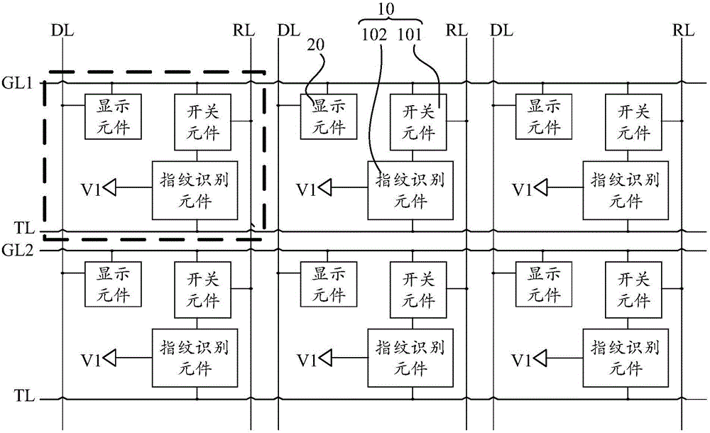
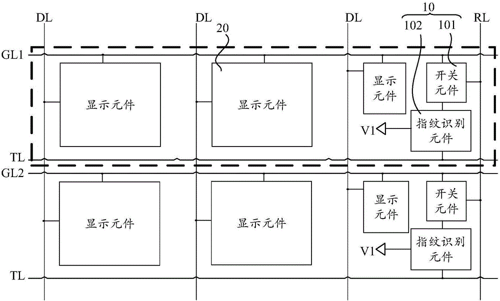
[0049] An embodiment of the present invention provides an array substrate, such as Figure 2(a) with 2(b) As shown, it includes a plurality of sub-pixels, at least one sub-pixel constitutes a repeating unit (dashed line box in FIG. 2 ), and one of the sub-pixels in the repeating unit includes the fingerprint recognition component 10 . Wherein, the fingerprint identification component 10 includes a fingerprint identification element 102 and a switch element 10...


PUM


Abstract

The embodiment of the invention provides an array substrate, a display device and a driving method for the display device, relates to the technical field of display, and can improve the fingerprint detection precision. The array substrate comprises a plurality of subpixels, and each subpixel comprises a display element. At least one subpixel forms one repetition unit, and one subpixel in the repetition unit also comprises a fingerprint recognition assembly, wherein the fingerprint recognition assembly comprises a fingerprint recognition element and a switching element. The switching element is controlled by a grid line to be started, so as to enable the fingerprint recognition unit to be connected with a reading signal line. The fingerprint recognition element is controlled by a first voltage end to collect fingerprint information, and is controlled by a transfer signal line to store the fingerprint information, so as to enable the fingerprint information to be transmitted to the reading signal line when the fingerprint recognition element is connected with the reading signal line. The display element is controlled by a grid line to be turned on or off, and a data signal is inputted to the display element through a data line when the display element is turned on. The array substrate is used for the display device with a function of fingerprint recognition.

Description

technical field [0001] The present invention relates to the field of display technology, in particular to an array substrate, a display device and a driving method thereof. Background technique [0002] Fingerprint is an innate, unique, fixed, and distinguishable identification feature of the human body, the most important of which is the feature of valleys and ridges. Fingerprint identification technology has the advantages of high precision, fast speed, low price, and high user acceptance, and has been widely used in the field of personal identity verification. [0003] At present, how to implement fingerprint recognition in the display area of ​​the display device is gradually being concerned, such as figure 1 Shown is a display device with a fingerprint recognition function, wherein the fingerprint recognition sensor is integrated in a sub-pixel of the display device. [0004] Specifically, each fingerprint sensor is composed of a photodiode L and a thin film transisto...

Claims


Application Information

Patent Timeline
Patent Type & Authority Applications(China)
IPC IPC(8): G06K9/00
CPCG06V40/1306
Inventor 丁小梁董学王海生陈小川刘英明刘伟王鹏鹏杨盛际李昌峰赵卫杰
Owner BOE TECH GRP CO LTD
Why Eureka
Try Eureka