Whole-board mounting device and method in the production of surface-mounted quartz crystal resonators

A technology for quartz crystals and resonators, which is applied in the field of whole-board mounting devices in the production of surface-mounted quartz crystal resonators. It can solve the problems of low production efficiency, large demand for coating fixtures, and slow circulation, etc., and achieves improved production efficiency and expansion. SMT throughput and the effect of increasing the SMT speed

Active Publication Date: 2019-04-26
SICHUAN MDH TECH CO LTD
View PDF6 Cites 0 Cited by
  • Summary
  • Abstract
  • Description
  • Claims
  • Application Information

AI Technical Summary

Problems solved by technology

[0007] 1. It takes about 0.6s to pick up and place a single wafer one by one, and 240s to transfer a whole board fixture (taking 400pcs as an example), and the production efficiency is low
[0008] 2. Due to low production efficiency and slow flow, the need for coating fixtures is large

Method used


Image

  • Whole-board mounting device and method in the production of surface-mounted quartz crystal resonators
  • Whole-board mounting device and method in the production of surface-mounted quartz crystal resonators
  • Whole-board mounting device and method in the production of surface-mounted quartz crystal resonators

Examples


Embodiment 1

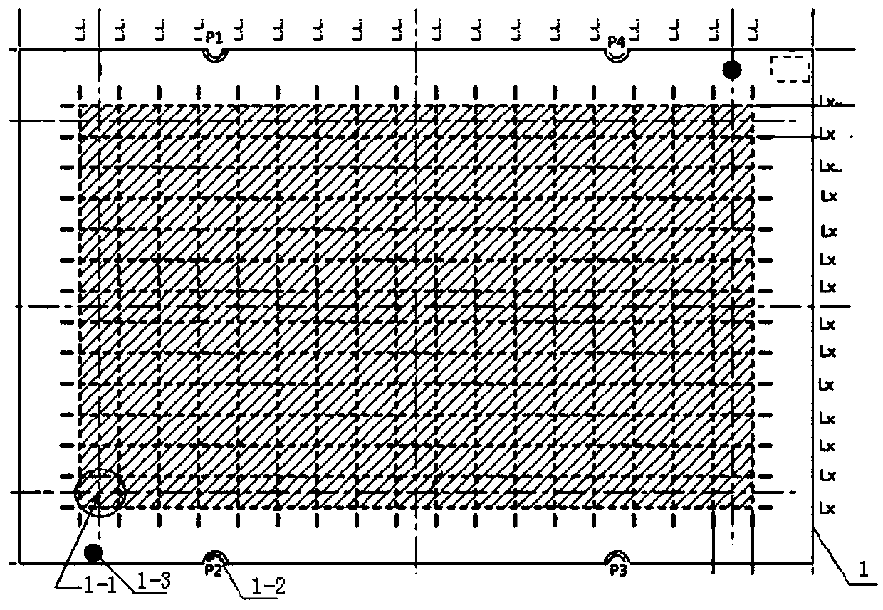
[0061] In this embodiment, the rows and columns of the entire wafer on the coating fixture are the same as the row and column spacing of the entire base, that is, after the primer coating process for all the monomer bases on the entire base is completed, all the monomer bases The seat is loaded with the film process at the same time. In this embodiment, the entire wafer on the coating fixture is a P*Q matrix, and the entire base is an M*N matrix, P=M, Q=N. When the entire base is After the left and right platforms of each monomer base are coated with primer, follow the steps below to move and place the entire wafer. The specific loading process is as follows:

[0062] Step 1. Place the entire wafer placed in the coating fixture into the wafer cage, the number of each wafer on the entire wafer, the number of suction nozzles in the suction box, and the number of single bases on the entire base be consistent;

[0063] Step 2. Install the coating fixture with the whole wafer in t...

Embodiment 2

[0069] In this embodiment, the process of moving the entire wafer on the coating jig to the entire base is similar to that of Embodiment 1, except that the array of wafers on the coating jig in this embodiment is the same as that of the entire base. The distance between rows and columns is twice, for the entire wafer on the coating fixture is a P*Q matrix, and the entire base is an M*N matrix, P=2M, Q=2N, that is, all the monomer substrates on the entire base are completed After the primer coating process of the base, the single base located on the entire board of the base with odd rows and columns or even rows and columns is simultaneously subjected to the chip loading process. In this embodiment, the single base with odd rows and odd columns on the entire base is selected first, and then the single base with even rows and even columns on the entire base is coated.

[0070] After the left and right platforms of each single base on the entire base board are coated with primer,...

Embodiment 3

[0079] In this embodiment, the process of moving the entire plate wafer on the coating fixture to the entire base plate is similar to Embodiment 1, the difference is that in this embodiment, the coating fixture is installed in the suction box, and the suction box is turned over. All done manually.

[0080] In addition, in this embodiment, the rows and columns of the entire wafer on the coating fixture are three times the row-column spacing of the entire base. For the entire wafer on the coating fixture, it is a P*Q matrix, and the entire base is an M*N matrix. P = 3M, Q = 3N, that is, after the primer coating process of all monomer bases on the entire base board is completed, the monomer bases on the entire base board separated by two rows and two columns are simultaneously applied. piece craft. Taking the 12*12 base board as an example, in this embodiment, the first, 4th, 7th, and 10th rows and 1st, 4th, 7th, and 10th rows of the base board are first selected. Put on the fi...


PUM


Abstract

The invention relates to the field of electronic devices, and specifically, to a full-array die attachment device and method utilized in producing a surface-mount quartz crystal oscillator. The full-array die attachment device comprises a fixing device, a suction device located in the fixing device, and a transfer device detachably connected to the fixing device. A full array of dies to be attached on a full array of substrate bases (1) are arranged on the transfer device. The full array of dies comprise a plurality of dies. The suction device is in contact with the full array of dies at the transfer device. The full-array die attachment method comprises: transferring a plurality of dies together to form a full array of dies, to enable each of the full array of dies to correspond to a single substrate base configured directly therebelow. A pick-up tool (10) having a coating film suctions the dies together, and then places, on a full array of substrate bases (1) after applying an adhesive dispensing process thereon, all of the dies, reducing the time for die placement, providing a fast die attachment process, increasing the production efficiency by ten to hundred times, and expanding a production volume.

Description

technical field [0001] The invention belongs to the field of electronic components, and in particular relates to a whole-board mounting device and method in the production of surface-mounted quartz crystal resonators. Background technique [0002] Quartz crystal resonator, also known as quartz crystal, commonly known as crystal oscillator, is a resonator made by using the piezoelectric effect of quartz crystal. It can be used together with semiconductor devices and resistance-capacitance components to form a quartz crystal oscillator. [0003] Quartz wafer, hereinafter referred to as wafer, it can be square, rectangular or circular, etc., coated with silver layer on its two corresponding surfaces as electrodes, surface-mounted quartz crystal resonator is the electrode on the quartz wafer through conductive glue Conduct electrical connection with the base, apply primer on the base to form conductive adhesive under the quartz wafer, place the quartz wafer above the primer, and...

Claims


Application Information

Patent Timeline
Patent Type & Authority Patents(China)
IPC IPC(8): H03H3/02H03H9/19
CPCH03H3/02H03H9/19
Inventor 黄屹李斌
Owner SICHUAN MDH TECH CO LTD
Why Eureka
Try Eureka