Control method and system in semiconductor processing process

A processing and control system technology, applied in semiconductor/solid-state device manufacturing, electrical components, circuits, etc., can solve the problems of measurement data growth, occupation of host processing resources, etc., and achieve the effect of improving production efficiency and reducing the burden of data processing

Active Publication Date: 2016-12-07
SEMICON MFG INT (SHANGHAI) CORP
View PDF5 Cites 10 Cited by
  • Summary
  • Abstract
  • Description
  • Claims
  • Application Information

AI Technical Summary

Problems solved by technology

Among them, almost every step of the movement of the silicon chip needs to be confirmed by the host, which will occupy the processing resources of the host
Especially when the semiconductor process enters 20nm and below, the measurement data will increase exponentially, and this situation will be even more serious

Method used


Image

  • Control method and system in semiconductor processing process
  • Control method and system in semiconductor processing process
  • Control method and system in semiconductor processing process

Examples


Embodiment Construction

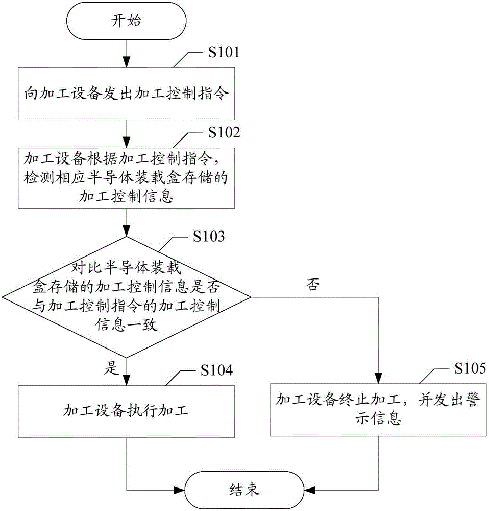
[0052] The information management method of the existing integrated circuit manufacturing plant is that a server, or host, is responsible for the management and processing of silicon chips and the management of processing equipment, that is, the information management method in which the host dominates everything, or is called "master-slave". model". The host manages and processes silicon wafers and the management of processing equipment, including all necessary processes in the process of silicon wafer processing, as well as the storage, processing, and feed-forward of programs and data required for silicon wafer processing after data is collected by related equipment and feedback etc. Among them, almost every movement of the silicon chip needs to be confirmed by the host, which will occupy the processing resources of the host. Especially when the semiconductor process enters 20nm and below, the measurement data will increase exponentially, and this situation will become mor...


PUM


Abstract

The invention discloses a control method and system in a semiconductor processing process. The method comprises the following steps: emitting a processing control instruction to a processing device; the processing device, according to the processing control instruction, detecting processing control information stored by a corresponding semiconductor loading box; the processing device comparing whether the processing control information of the semiconductor loading box is consistent with the processing control information of the processing control instruction; in case that the processing control information of the semiconductor loading box is consistent with the processing control information of the processing control instruction, the processing device executing processing; and in case that the processing control information of the semiconductor loading box is not consistent with the processing control information of the processing control instruction, the processing device terminating processing, and emitting alarm information. Through the method and system, fewer resources at a host end can be occupied in the processing process of a semiconductor product.

Description

technical field [0001] The invention relates to the technical field of semiconductor manufacturing, in particular to a control method and system in the semiconductor processing process. Background technique [0002] The information management method of the existing integrated circuit manufacturing plant is that a server, or host, is responsible for the management and processing of silicon chips and the management of processing equipment, that is, the information management method in which the host dominates everything, or is called "master-slave". model". The host manages and processes silicon wafers and the management of processing equipment, including all necessary processes in the process of silicon wafer processing, as well as the storage, processing, and feed-forward of programs and data required for silicon wafer processing after data is collected by related equipment and feedback etc. Among them, almost every movement of the silicon chip needs to be confirmed by the...

Claims


Application Information

Patent Timeline
Patent Type & Authority Applications(China)
IPC IPC(8): H01L21/67
Inventor 伍强郝静安刘畅胡华勇蒋运涛
Owner SEMICON MFG INT (SHANGHAI) CORP
Why Eureka
Try Eureka