

Top-emitting full-color organic light-emitting display device and preparation method thereof
A technology for light-emitting display devices and organic light-emitting devices, which is applied in the manufacturing of semiconductor/solid-state devices, electric solid-state devices, semiconductor devices, etc., can solve the problem of high production cost of OLED devices, simplify the preparation process, solve the complex processing technology, and reduce costs. Effect
- Summary
- Abstract
- Description
- Claims
- Application Information
AI Technical Summary
Benefits of technology
Problems solved by technology
Method used
Image


Examples
Embodiment 1
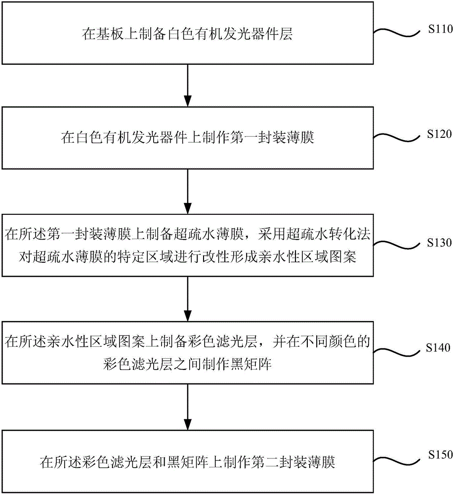
[0041] figure 1 It is a flow chart of a method for preparing a top-emitting full-color organic light-emitting display device provided in Embodiment 1 of the present invention, figure 2 It is a top-emitting full-color organic light-emitting display device made by the method according to claim 1. see figure 1 and figure 2 , the method of this embodiment includes the following steps:
[0042] Step 110 , preparing a white organic light emitting device layer 2 on the substrate 1 , specifically, the above white organic light emitting device layer 2 may include a thin film transistor pixel driving array 21 and a white organic light emitting device 22 .
[0043] In Embodiment 1 of the present invention, the above-mentioned thin film transistor pixel driving array 21 and white organic light emitting device 22 can be sequentially prepared on the substrate 1, wherein optionally, when preparing the thin film transistor pixel driving array 21, the driving circuit 23 can be prepared at...
Embodiment 2
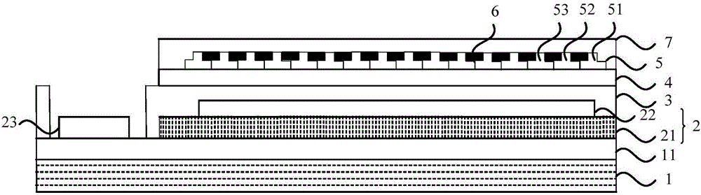
[0054] Embodiment 2 of the present invention mainly describes the technical scheme of modifying a specific region of a super-hydrophobic film by ultraviolet light irradiation to form a hydrophilic region pattern, and then preparing a color filter layer. Top-emission full-color organic light-emitting display devices The preparation method is described in detail. see Figure 4-10 , the method of this embodiment includes the following steps:
[0055] Step 1. Prepare buffer layer 11 on substrate 1. For details, please refer to image 3 As shown, 300nm SiO can be deposited using PECVD (Plasma Enhanced Chemical Vapor Deposition, plasma enhanced chemical vapor deposition method) 2 as buffer layer 11.
[0056] Step 2, prepare thin film transistor pixel driving array 21 and driving circuit 23 on buffer layer 11, specifically, refer to Figure 4 shown.
[0057] Step 3, on the thin film transistor pixel driving array 21, make a white organic light-emitting device 22 by vapor deposit...
Embodiment 3
[0073] Embodiment 3 of the present invention is a further optimization on the basis of Embodiment 1 above. image 3 It is a flowchart of a method for manufacturing a top-emission full-color organic light-emitting display device provided in Embodiment 3 of the present invention. In the embodiment of the present invention, the specific region of the super-hydrophobic film 4 is modified by the stamp transfer method to form a hydrophilic region pattern and then the color filter layer 5 is prepared as an example, and the method for preparing a top-emitting full-color organic light-emitting display device for details. see Figure 4-11 , the method of this embodiment includes the following steps:
[0074] Steps 1-4 and steps 6-8 can refer to Embodiment 2, and will not be repeated here
[0075] Step 5. Prepare a super-hydrophobic film 4 on the first encapsulation film 3, and use a stamp transfer method to modify a specific area of the super-hydrophobic film 4 to form a hydrophili...
PUM
| Property | Measurement | Unit |
|---|---|---|
| Thickness | aaaaa | aaaaa |
| Thickness | aaaaa | aaaaa |
Abstract
Description
Claims
Application Information