Optical communication device

A communication device and optical technology, applied in the field of optical communication, can solve problems such as unfavorable cost saving, increase the number of optical fibers, etc., and achieve the effects of increasing the data transmission volume, reducing the number and reducing the cost

Inactive Publication Date: 2017-01-04
HONG FU JIN PRECISION IND (SHENZHEN) CO LTD +1
View PDF0 Cites 6 Cited by
  • Summary
  • Abstract
  • Description
  • Claims
  • Application Information

AI Technical Summary

Problems solved by technology

However, these optical communication devices often only involve coupling an optical signal from an optical signal emitting source to the optical fiber. Since an optical signal emitting source can only emit an optical signal of one color, the optical fiber is only used for transmitting one light signals of different colors
To realize the transmission of optical signals of different colors, it is often necessary to increase the number of optical fibers, which is not conducive to cost saving

Method used


Image

  • Optical communication device
  • Optical communication device
  • Optical communication device

Examples


Embodiment Construction

[0020] The heat dissipation plate provided by the technical solution and its manufacturing method will be further described in detail below with reference to the drawings and embodiments.

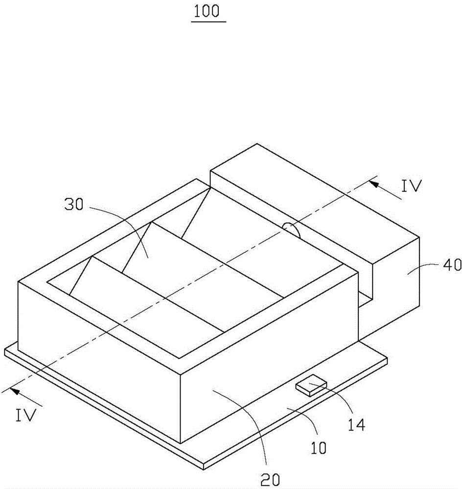
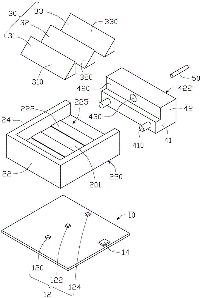
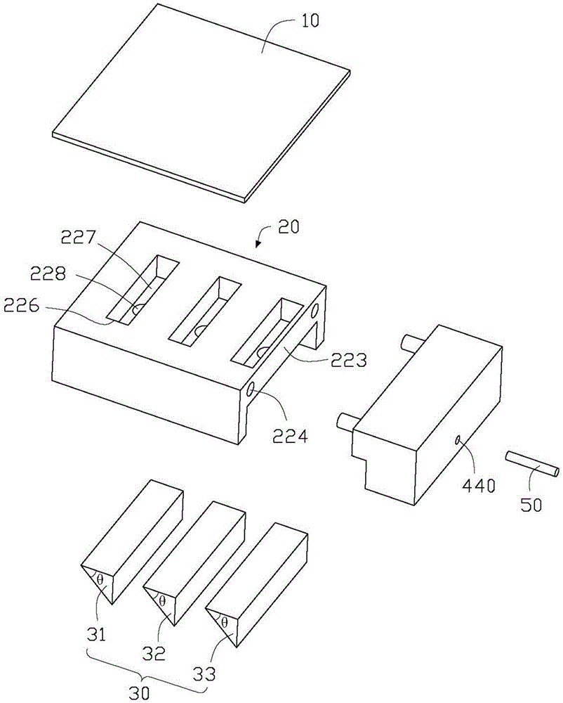
[0021] figure 1 , figure 2 An optical communication device 100 provided in the first embodiment of the technical solution. The optical communication device 100 includes a circuit board 10 , a first optical coupling module 20 , an optical deflection module 30 , a second optical coupling module 40 , and an optical fiber 50 .

[0022] The circuit board 10 is provided with a plurality of light emitting elements 12 capable of emitting light signals of different colors and a control chip 14 . The light emitting element 12 is a laser diode (Laser Diode). In this embodiment, the light emitting element 12 includes a first light emitting element 120 , a second light emitting element 122 and a third light emitting element 124 . The first light-emitting element 120 , the second light-emitting elem...


PUM


Abstract

The present invention provides an optical communication device. The device comprises a circuit board, a first optical coupling module, a light deflection module and a second optical coupling module. The circuit board is provided with a plurality of light emission elements capable of emitting different colors. The first optical coupling module includes a plurality of first optical coupling lenses arranged in order and being in one-to-one correspondence with each light emission element. The light deflection module includes a plurality of light deflection portions arranged in order, and each light deflection portion corresponds to one light emission element; each first deflection portion in the deflection portions includes a first reflection surface, and the other deflections in the deflection portions include color separation surfaces; the first reflection surfaces reflect optical signals of the first optical coupling lens corresponding to the first reflection surface, and each color separation surface reflects the light of the first optical coupling lens corresponding to the color separation surface and transmits the optical signals being incident from one light deflection portion; and the second optical coupling module includes a second optical coupling lens and fibers, and the second optical coupling lens is configured to perform coupling of the optical signals from the light deflection module and enter the fibers.

Description

technical field [0001] The invention relates to the technical field of optical communication, in particular to an optical communication device. Background technique [0002] In the field of optical communication technology, an optical communication device generally includes an optical signal transmitting source, an optical coupling lens, and an optical fiber. The optical signal emitted by the optical signal transmitting source is coupled to the optical fiber by the optical coupling lens, thereby realizing the transmission of the optical signal. . However, these optical communication devices often only involve coupling an optical signal from an optical signal emitting source to the optical fiber. Since an optical signal emitting source can only emit an optical signal of one color, the optical fiber is only used for transmitting one light signals of different colors. To realize the transmission of optical signals of different colors, it is often necessary to increase the num...

Claims


Application Information

Patent Timeline
Patent Type & Authority Applications(China)
IPC IPC(8): G02B6/42G02B6/43H04B10/50
CPCG02B6/4204G02B6/4214G02B6/43H04B10/501G02B6/4231G02B6/4215G02B6/4212G02B6/29362
Inventor 张仁淙
Owner HONG FU JIN PRECISION IND (SHENZHEN) CO LTD
Why Eureka
Try Eureka