Chip wireless debugging circuit and method

A technology for debugging circuits and debugging methods, which is used in electronic circuit testing, electrical measurement, and electrical variable measurement. Effects of Vulnerability Issues

Active Publication Date: 2019-04-02
FUZHOU ROCKCHIP SEMICON
View PDF6 Cites 0 Cited by
  • Summary
  • Abstract
  • Description
  • Claims
  • Application Information

AI Technical Summary

Problems solved by technology

However, an important problem currently restricting IoT chip devices is that all devices and basic chips still rely on traditional physical electrical devices, such as power sockets, debugging sockets, etc. Work in liquid environments such as swimming or bathing or other harsh environments
However, with the development of technology, some chips that do not require physical connection have appeared, but the verification and testing of these chips has become a difficult problem
[0003] Therefore, the present invention proposes a debugging circuit and method, which can debug the chip without physical connection, which greatly supports and improves the production and development process of chips without physical electrical interfaces. At the same time, if the debugging circuit or method Used on traditional chips, it can also simplify the complexity of test equipment design, and can also solve the vulnerability problem of physical connection equipment

Method used


Image

  • Chip wireless debugging circuit and method
  • Chip wireless debugging circuit and method
  • Chip wireless debugging circuit and method

Examples


Embodiment Construction

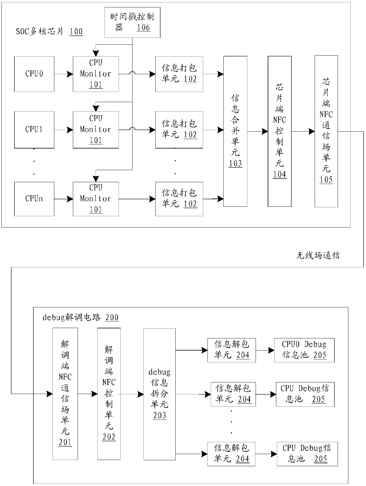
[0033] see figure 1 As shown, the chip of the present invention includes an on-chip circuit 100 and a debug demodulation circuit 200;

[0034] The on-chip circuit 100 includes a plurality of CPUs, a plurality of CPU monitors 101, a plurality of information packaging units 102, an information merging unit 103, a chip-side NFC control unit 104, a chip-side NFC communication field unit 105 and a time stamp controller 106 ; The plurality of CPUs, the plurality of CPU monitors 101, and the plurality of information packing units 102 are sequentially connected one by one, and the plurality of information packing units 102 are all connected to the information combining unit 103, and the information combining unit 103, The chip-side NFC control unit 104 and the chip-side NFC communication field unit 105 are connected sequentially; the time stamp controller 106 is connected to a plurality of CPU monitors 101 respectively;

[0035] The debug demodulation circuit 200 includes a demodulat...


PUM


Abstract

The invention provides a wireless debugging circuit and method for a chip, and the circuit comprises a chip internal circuit and a debug demodulation circuit. The chip internal circuit comprises a plurality of CPUs, a plurality of CPU monitors, a plurality of information packaging units, an information merging unit, a chip end NFC control unit, a chip end NFC communication field unit, and a time stamp controller. The debug demodulation circuit comprises a demodulation end NFC communication field unit, a demodulation end NFC control unit, a debug information splitting unit, a plurality of information unpacking units, and a plurality of CPU debug information pools. The circuit can complete the communication connection in the whole debugging process only if the NFC communication field of the debug demodulation circuit gets close to the NFC communication field of the chip, and there is no need of a physical electrical interface of the chip for wiring.

Description

technical field [0001] The invention relates to a chip wireless debugging circuit and method. Background technique [0002] With the rapid development of SOC chip technology, the Internet of Things technology is becoming more and more important. However, an important problem currently restricting IoT chip devices is that all devices and basic chips still rely on traditional physical electrical devices, such as power sockets, debugging sockets, etc. Work in liquid environments such as swimming or bathing or other harsh environments. However, with the development of technology, there have been some chips that do not require physical connection, but the verification and testing of these chips has become a difficult problem. [0003] Therefore, the present invention proposes a debugging circuit and method, which can debug the chip without physical connection, which greatly supports and improves the production and development process of chips without physical electrical interfa...

Claims


Application Information

Patent Timeline
Patent Type & Authority Patents(China)
IPC IPC(8): G01R31/28
CPCG01R31/2851
Inventor 廖裕民
Owner FUZHOU ROCKCHIP SEMICON
Why Eureka
Try Eureka