

Wireless testing circuit and method for chip
A technology of wireless testing and wireless charging, which is applied in the field of testing circuits, can solve problems such as equipment failure, difficulty in chip verification and testing, and dependence on physical electricity, etc., to simplify testing equipment, improve production and development processes, and solve vulnerability problems Effect
- Summary
- Abstract
- Description
- Claims
- Application Information
AI Technical Summary
Problems solved by technology
Method used
Image

Examples
Embodiment Construction
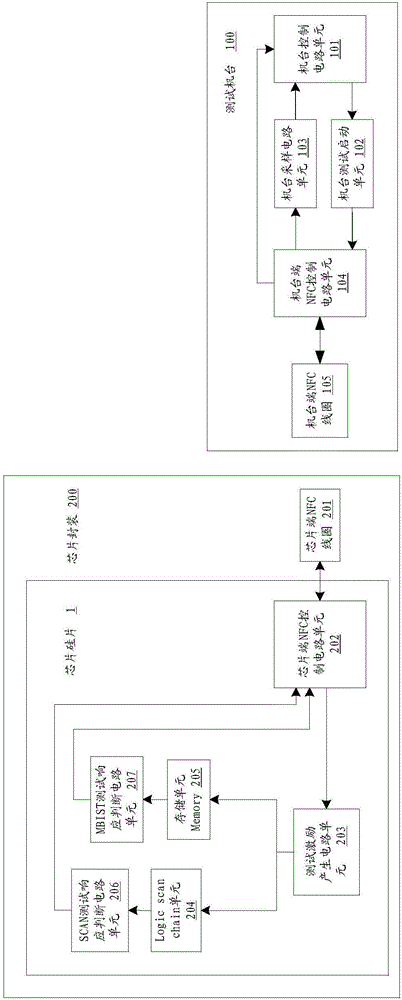
[0034] see figure 1 As shown, the wireless test circuit of the chip of the present invention includes a test machine circuit 100 and an on-chip circuit 200;
[0035] The test machine circuit 100 includes a machine control circuit unit 101, a machine test start unit 102, a machine sampling circuit unit 103, a machine end NFC control circuit unit 104 and a machine end NFC coil 105; the machine control circuit unit 101 is connected to the machine end NFC control circuit unit 104 through the machine test start unit 102 and the machine sampling circuit unit 103 respectively, and the machine end NFC control circuit unit 104 is connected to the machine end NFC coil 105, and the The machine control circuit unit 101 is also connected to the machine end NFC control circuit unit 104;
[0036]The on-chip circuit 200 includes a chip-side NFC coil 201, a chip-side NFC control circuit unit 202, a test excitation generating circuit unit 203, a logic_scan_chain unit 204, a storage unit Memory...
PUM
 Abstract
Description
Claims
Application Information