
A field limiting ring termination structure of a power semiconductor device

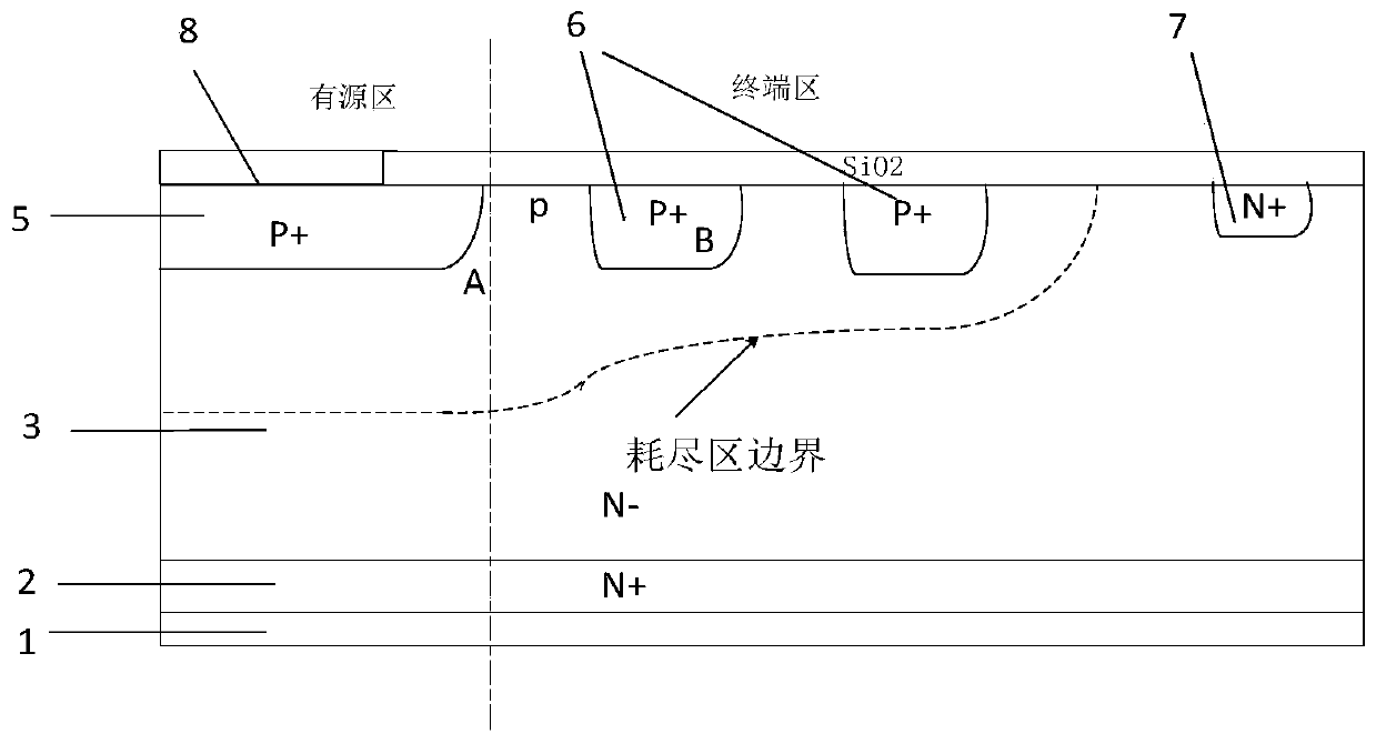
A power semiconductor and terminal structure technology, applied in the direction of semiconductor devices, electrical components, circuits, etc., can solve the problem of large occupied area, achieve the effect of alleviating the concentration of electric field and reducing the lateral area

Active Publication Date: 2019-11-29
UNIV OF ELECTRONICS SCI & TECH OF CHINA
View PDF3 Cites 0 Cited by
  • Summary
  • Abstract
  • Description
  • Claims
  • Application Information

AI Technical Summary

Problems solved by technology

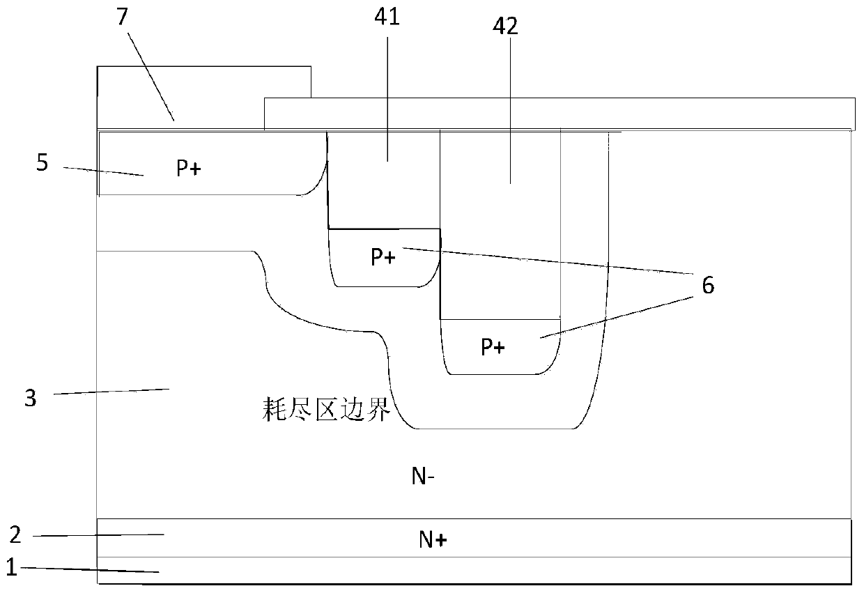
[0005] What the present invention aims to solve is to solve the problem that the existing field-limiting ring terminal structure occupies a large area, and propose a new stepped-shaped field-limiting ring terminal structure. Folding towards the inside of the device, reducing the terminal area and improving the terminal efficiency

Method used


Image

  • A field limiting ring termination structure of a power semiconductor device
  • A field limiting ring termination structure of a power semiconductor device
  • A field limiting ring termination structure of a power semiconductor device

Examples


Embodiment Construction

[0017] Below in conjunction with accompanying drawing, describe technical scheme of the present invention in detail:

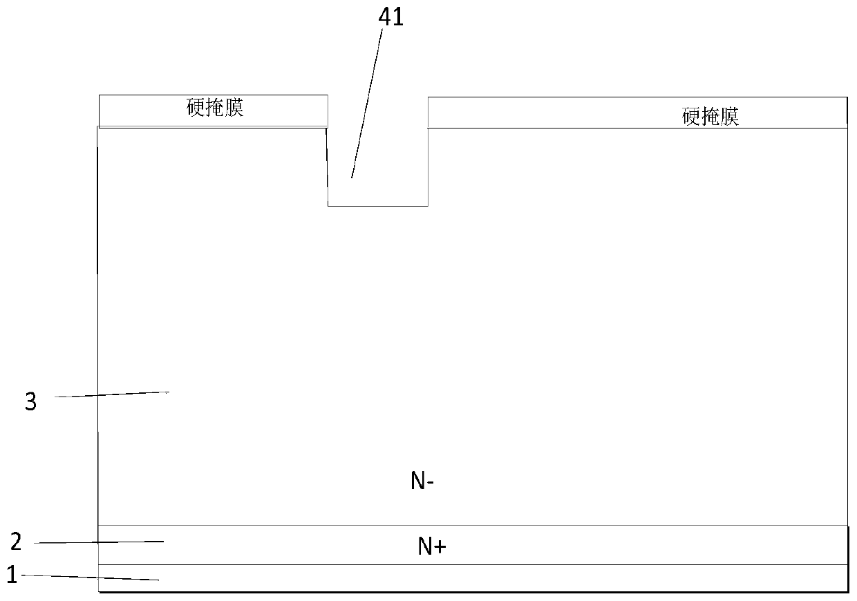
[0018] Such as figure 2 As shown, a field limiting ring terminal structure of a power semiconductor device includes a heavily doped semiconductor substrate 2 of the first conductivity type, and a semiconductor of the first conductivity type located on the upper surface of the heavily doped semiconductor substrate 2 of the first conductivity type The lightly doped drift region 3 and the metal drain electrode 1 located on the lower surface of the first conductivity type semiconductor heavily doped substrate 2 . The doped region 5 of the second conductivity type semiconductor in the lightly doped drift region 3 of the first conductivity type semiconductor located in the active region of the device, the second conductivity type semiconductor doped region 5 and the first conductivity type semiconductor The lightly doped drift region 3 forms a main junction, and t...


PUM


Abstract

The invention belongs to the technical field of manufacturing a semiconductor power device and especially relates to a field limiting ring terminal structure for a power semiconductor device. Two or more grooves in different thicknesses are arranged in a terminal area of the terminal structure; the grooves are tightly connected; same insulating media fill the grooves; an upper side wall of the groove in the minimal thickness is adjacent to a main structure of an active area; the bottoms of the grooves are doped, so as to form a floating field ring in the terminal area. According to the invention, a floating field ring structure at a horizontal interval is folded toward the interior of the device, so that the thickness of the shifting area in the device can be fully utilized, the cross area of the terminal can be further reduced and the use efficiency of the terminal can be increased.

Description

technical field [0001] The invention belongs to the technical field of semiconductor power device preparation, and in particular relates to a field-limiting ring terminal structure of a power semiconductor device and a manufacturing method thereof. Background technique [0002] When the PN junction is manufactured by the actual planar process, since the impurities not only diffuse vertically from the surface to the inside, but also diffuse laterally along the horizontal direction, a cylindrical junction is formed at the edge of the diffusion window, and a cylindrical junction is formed at the four corners of the rectangular diffusion window. spherical knot. The junction bending has a great influence on the breakdown characteristics of the PN junction. Under a certain voltage, the electric field strength that varies with distance is more concentrated at the junction bending, where the breakdown critical point can be reached at a lower reverse voltage. Breakdown of the electr...

Claims


Application Information

Patent Timeline
Patent Type & Authority Patents(China)
IPC IPC(8): H01L29/06
CPCH01L29/0619
Inventor 任敏包惠萍林育赐谢驰李家驹李泽宏张波
Owner UNIV OF ELECTRONICS SCI & TECH OF CHINA
Learn More