A foldable terminal with an internal field plate

A folding type, field plate technology, applied in semiconductor devices, electrical components, circuits, etc., can solve the problems of rising device cost and large occupation area, and achieve the effect of alleviating electric field concentration and reducing lateral area

Inactive Publication Date: 2020-09-29
UNIV OF ELECTRONICS SCI & TECH OF CHINA
View PDF6 Cites 2 Cited by
  • Summary
  • Abstract
  • Description
  • Claims
  • Application Information

AI Technical Summary

Problems solved by technology

Therefore, in high-voltage devices, the area occupied by the existing extended terminal structure is too large, resulting in an increase in device cost

Method used


Image

  • A foldable terminal with an internal field plate
  • A foldable terminal with an internal field plate
  • A foldable terminal with an internal field plate

Examples


Embodiment 1

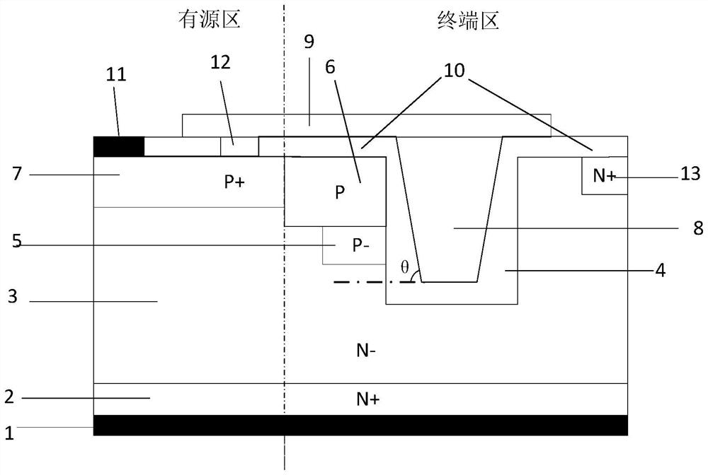
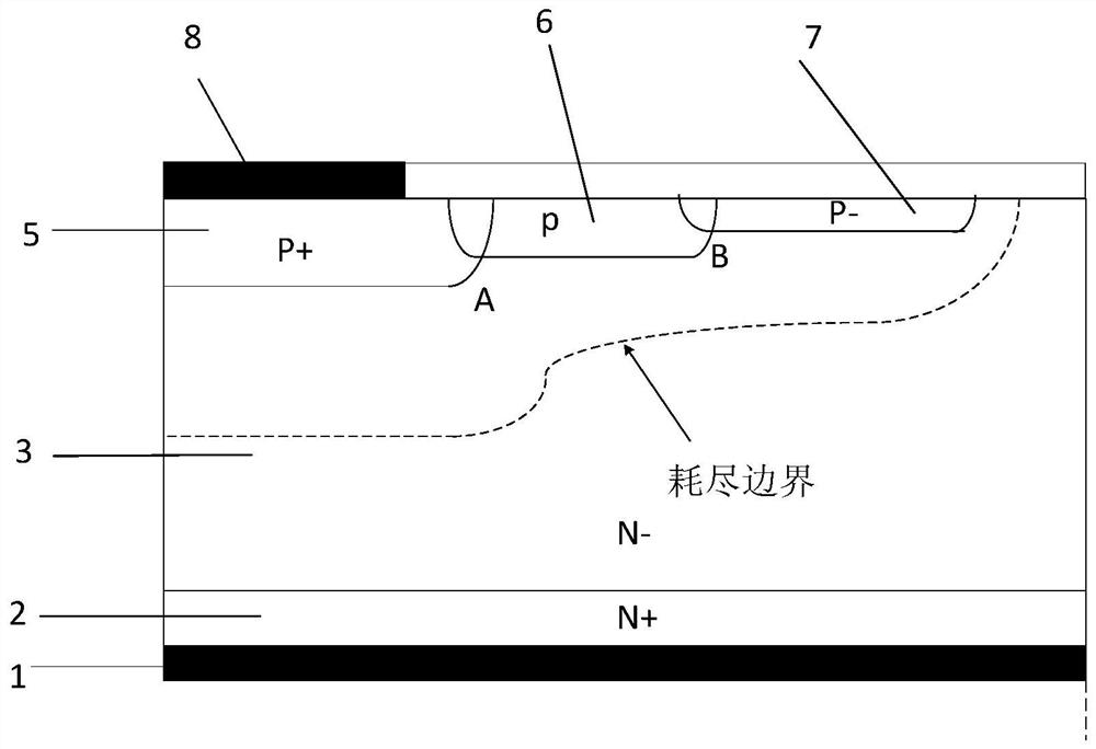
[0032] Such as figure 1 As shown, the termination structure with internal field plates in this example includes a heavily doped semiconductor substrate 2 of the first conductivity type, a lightly doped semiconductor substrate of the first conductivity type located on the upper surface of the heavily doped semiconductor substrate 2 The drift region 3 and the metal drain electrode 1 located on the lower surface of the heavily doped semiconductor substrate 2 of the first conductivity type; it is characterized in that there is a groove 4 in the lightly doped semiconductor drift region 3 of the first conductivity type, and the groove The groove 4 is located in the middle of the lightly doped semiconductor drift region 3 of the first conductivity type, and extends vertically downward into the lightly doped drift region 3 of the semiconductor of the first conductivity type along the upper surface of the lightly doped semiconductor drift region 3 of the first conductivity type, so The...

Embodiment 2

[0049] Such as Figure 10 As shown, the structure of this example is based on Example 1, adding a buried layer 14 of the second conductivity type semiconductor material directly below the trench 4, which can slow down the electric field concentration at the corner of the trench and further improve the withstand voltage capability .

Embodiment 3

[0051] Such as Figure 11 As shown, the structure of this example is that on the basis of Embodiment 1, a lightly doped region 14 of the second conductivity type with a lower doping concentration is formed along the sidewall directly under the implantation region 5 of the second conductivity type, which can Enhance the effect of JTE.


PUM


Abstract

A folded terminal with a field plate in the body, which folds the field plate structure and the junction terminal extension area toward the inside of the device, making full use of the thickness of the drift region in the body, thereby reducing the lateral area of ​​the terminal, and alleviating the electric field concentration at the PN junction termination end and breakdown The position of the point is transferred from the terminal end of the original PN junction to the body, and the withstand voltage of the terminal can reach the breakdown voltage of the parallel plane junction. This structure can obtain a smaller area than the conventional structure under the condition of the same withstand voltage.

Description

technical field [0001] The invention belongs to the technical field of semiconductors and relates to a folded terminal structure with internal field plates. Background technique [0002] The ability of a power device to block high voltage mainly depends on the reverse bias breakdown voltage of a specific PN junction in the device structure. The size of all semiconductor devices is limited, and the wafer is cut into chips and packaged to make devices. The crystal lattice of the silicon wafer will be greatly damaged during the cutting process. For power devices, if the cut passes through regions of the device structure that are subjected to high voltages, lattice damage can cause large leakage currents, which can reduce the breakdown voltage and long-term stability of the device. In power devices, due to the influence of PN junction bending or surface non-ideal factors at the termination of PN junction, the reverse bias PN junction breakdown voltage is limited to occur near ...

Claims


Application Information

Patent Timeline
Patent Type & Authority Patents(China)
IPC IPC(8): H01L29/78
CPCH01L29/7811H01L29/7823H01L29/0638H01L29/0615H01L29/407H01L29/7813H01L29/78
Inventor 任敏张玉蒙底聪熊景枝李泽宏张金平高巍张波
Owner UNIV OF ELECTRONICS SCI & TECH OF CHINA
Why Eureka
Try Eureka