

Dynamic random access memory and fabrication thereof
A dynamic random access and storage unit technology, which is applied in semiconductor/solid-state device manufacturing, electrical components, transistors, etc., can solve the problems of increasing the integration of dynamic random access memory components, increasing the surface area of capacitors, difficult capacitors, etc., to achieve Improve storage capacity, increase integration, high integration effect
- Summary
- Abstract
- Description
- Claims
- Application Information
AI Technical Summary
Problems solved by technology
Method used
Image

Examples
Embodiment Construction
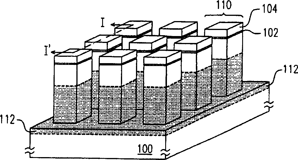
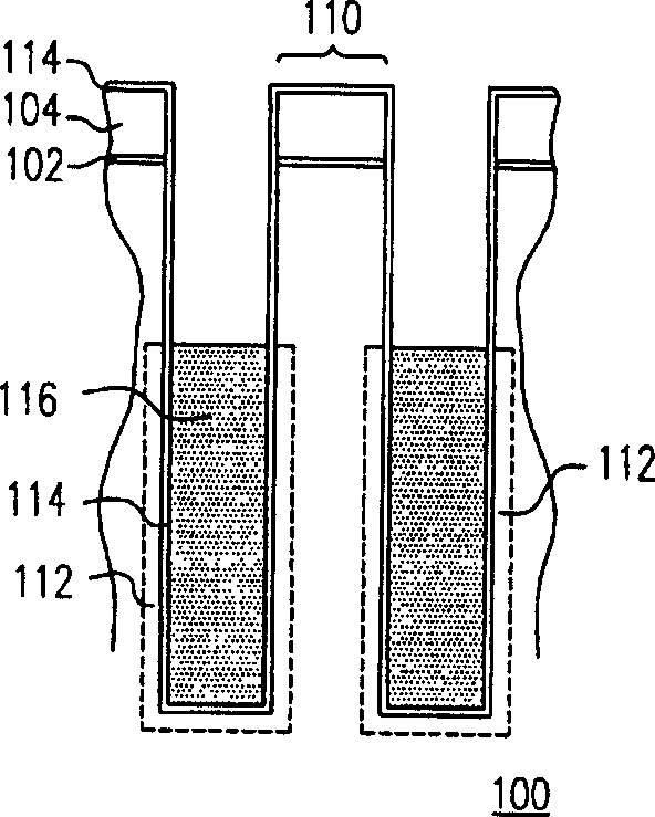
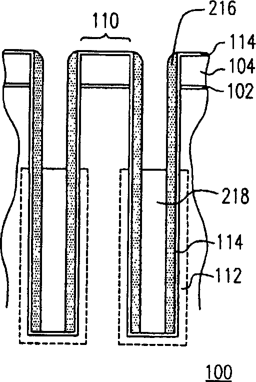
[0044] Figure 1 to Figure 16 It is a flow chart illustrating the fabrication of a dynamic random access memory (Dynamic Random Access Memory, DRAM) array according to a preferred embodiment of the present invention. figure 1 A perspective view clearly showing the arrangement of this DRAM array, Figure 2 to Figure 9 , Figure 11 to Figure 13 as well as Figure 16 (a) is figure 1 The cross-sectional view of the I-I′ site, and Figure 16 (b) then figure 1 Another cross-sectional view of the I-I' site. Figure 10 , Figure 14 as well as Figure 15 is the top view.
[0045] To put it more concretely, the figure 1 6 is a flowchart illustrating the fabrication of capacitors for DRAM arrays, Figure 7 to Figure 12 is a flow chart showing the fabrication of vertical transistors for DRAM arrays, and Figure 13 to Figure 16 It is a manufacturing flow diagram illustrating a subsequent manufacturing process, including a manufacturing flow diagram of a bit line and a word li...
PUM
 Abstract
Description
Claims
Application Information