Schottky diode based on n-type gallium oxide-p-type diamond and preparation method thereof
A Schottky diode and gallium oxide technology, applied in the field of microelectronics, can solve the problems of reduced device reliability, poor thermal conductivity, and obvious thermal effects, and achieve the effects of suppressing the electric field concentration effect, improving heat dissipation performance, and high terminal efficiency.
- Summary
- Abstract
- Description
- Claims
- Application Information
AI Technical Summary
Problems solved by technology
Method used
Image
Examples
Embodiment 1
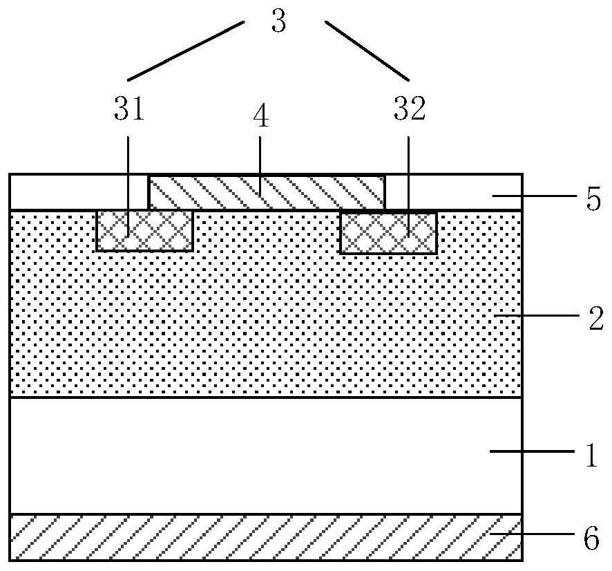
[0036] See figure 1 , figure 1 A schematic structural diagram of a Schottky diode based on n-type gallium oxide-p-type diamond provided in an embodiment of the present invention. The Schottky diode includes an n-type gallium oxide substrate 1 , an n-type gallium oxide epitaxial layer 2 , a p-type diamond junction region 3 , an anode 4 , an insulating medium 5 and a cathode 6 .
[0037] Specifically, the cathode 6, the n-type gallium oxide substrate 1, and the n-type gallium oxide epitaxial layer 2 are stacked in sequence. The p-type diamond junction regions 3 are distributed in the surface layer of the n-type gallium oxide epitaxial layer 2 to form a terminal structure. The anode 4 is located on the n-type gallium oxide epitaxial layer 2 , and two ends of the anode 4 partially overlap with the p-type diamond junction region 3 respectively. The insulating medium 5 is located on the n-type gallium oxide epitaxial layer 2 and is in contact with both ends of the anode 4 .
[0...
Embodiment 2
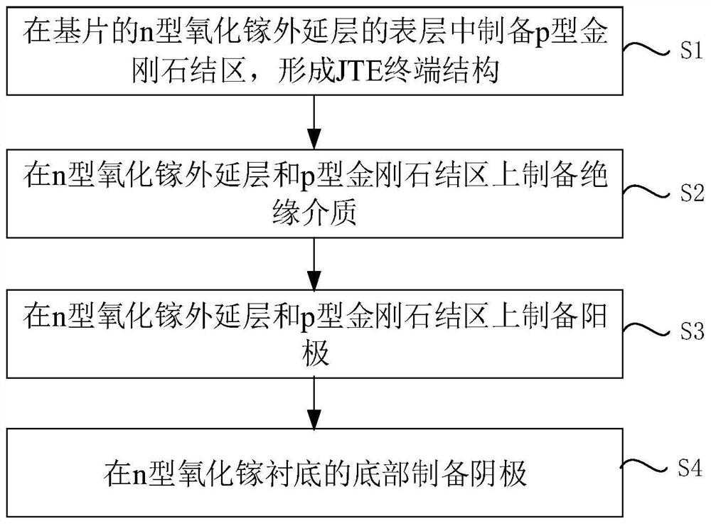
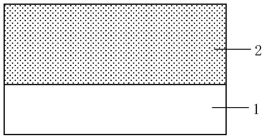
[0048] On the basis of Example 1, please refer to figure 2 and Figures 3a-3f , figure 2 A schematic flowchart of a method for preparing a Schottky diode based on n-type gallium oxide-p-type diamond provided in an embodiment of the present invention, Figures 3a-3f A process schematic diagram of a method for preparing a Schottky diode based on n-type gallium oxide-p-type diamond provided in an embodiment of the present invention.
[0049] The preparation method includes the steps:
[0050] S1. Prepare a p-type diamond junction region 3 in the surface layer of the n-type gallium oxide epitaxial layer 2 of the substrate to form a JTE terminal structure, wherein the substrate includes an n-type gallium oxide substrate 1 and an n-type gallium oxide substrate 1 2 on the n-type gallium oxide epitaxial layer. Include steps:
[0051] S11 , etching the n-type gallium oxide epitaxial layer 2 to form a junction groove 30 .
[0052] First, an epitaxial substrate is obtained. The e...
PUM
| Property | Measurement | Unit |
|---|---|---|
| thickness | aaaaa | aaaaa |
| thickness | aaaaa | aaaaa |
| thickness | aaaaa | aaaaa |
Abstract
Description
Claims
Application Information


