Display substrate and manufacturing method thereof
A technology for display substrates and manufacturing methods, applied in the fields of nonlinear optics, instruments, optics, etc., can solve the problems of uneven display of display panels, achieve the effects of improving display unevenness, reducing complexity, and simplifying the manufacturing process
- Summary
- Abstract
- Description
- Claims
- Application Information
AI Technical Summary
Problems solved by technology
Method used
Image

Examples
Embodiment Construction
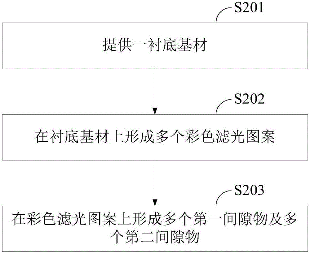
[0023] The following will clearly and completely describe the technical solutions in the embodiments of the present invention in conjunction with the accompanying drawings in the embodiments of the present invention. Obviously, the described embodiments are only some of the embodiments of the present invention, not all of them. Based on the embodiments of the present invention, all other embodiments obtained by persons of ordinary skill in the art without making creative efforts belong to the protection scope of the present invention.
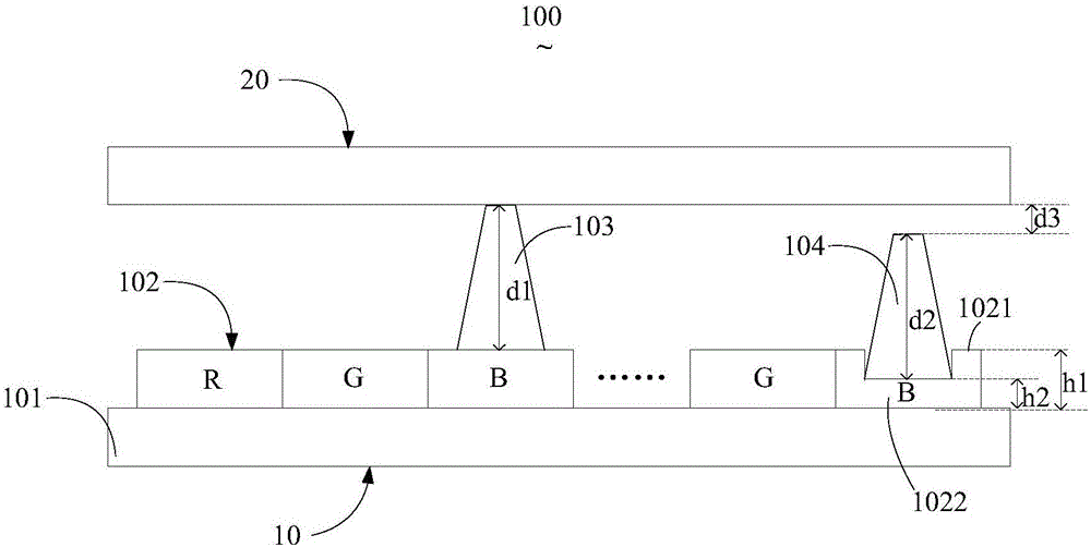
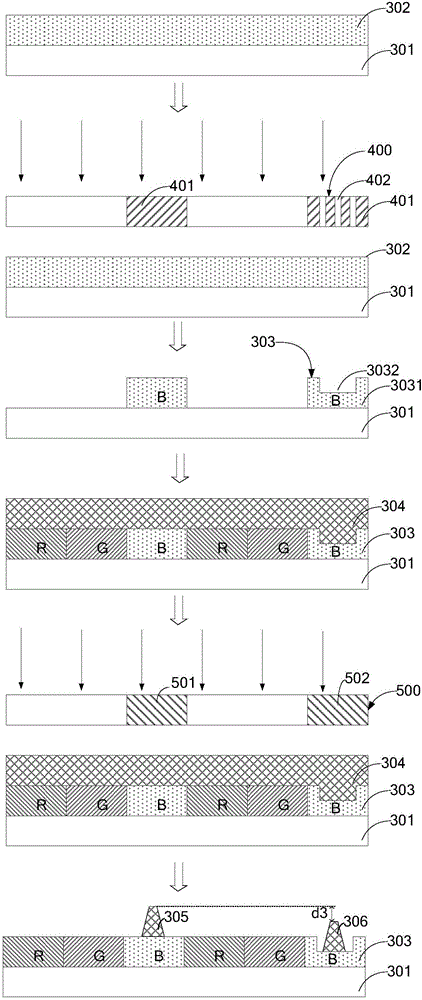
[0024] Please see figure 1 , figure 1 It is a structural cross-sectional view of a display substrate according to an embodiment of the present invention. Such as figure 1 As shown, the display substrate 10 of this embodiment includes a base material 101 , a plurality of color filter patterns 102 , a plurality of first spacers 103 and a plurality of second spacers 104 .
[0025] Wherein, a plurality of color filter patterns 102 are formed on ...
PUM
 Abstract
Description
Claims
Application Information
 - Generate Ideas
- Intellectual Property
- Life Sciences
- Materials
- Tech Scout
- Unparalleled Data Quality
- Higher Quality Content
- 60% Fewer Hallucinations
Browse by: Latest US Patents, China's latest patents, Technical Efficacy Thesaurus, Application Domain, Technology Topic, Popular Technical Reports.
© 2025 PatSnap. All rights reserved.Legal|Privacy policy|Modern Slavery Act Transparency Statement|Sitemap|About US| Contact US: help@patsnap.com