Supercharge Your Innovation With Domain-Expert AI Agents!

Display device, organic light emitting display panel and manufacturing method thereof

A technology of light-emitting display and manufacturing method, which is applied in semiconductor/solid-state device manufacturing, semiconductor devices, electrical components, etc., can solve problems such as adverse effects of organic light-emitting display panel display effects, signal crosstalk, etc., to increase spacing, improve design space, Increase the effect of the designable width

Active Publication Date: 2019-08-02
WUHAN TIANMA MICRO ELECTRONICS CO LTD +1
View PDF3 Cites 0 Cited by
  • Summary
  • Abstract
  • Description
  • Claims
  • Application Information

AI Technical Summary

Problems solved by technology

[0004] As the pixel density (Pixels Per Inch, PPI) of organic light-emitting display panels continues to increase, the number of display pixels required to be carried by the substrate 10 is also increasing, resulting in a gap between each display pixel and each display pixel. The distance between the included sub-pixels is getting smaller and smaller, so that the problem of signal crosstalk between adjacent sub-pixels is very easy to occur, which has a negative impact on the display effect of the organic light-emitting display panel.

Method used


Image

  • Display device, organic light emitting display panel and manufacturing method thereof
  • Display device, organic light emitting display panel and manufacturing method thereof
  • Display device, organic light emitting display panel and manufacturing method thereof

Examples


Embodiment Construction

[0031] The following will clearly and completely describe the technical solutions in the embodiments of the present invention with reference to the accompanying drawings in the embodiments of the present invention. Obviously, the described embodiments are only some, not all, embodiments of the present invention. Based on the embodiments of the present invention, all other embodiments obtained by persons of ordinary skill in the art without making creative efforts belong to the protection scope of the present invention.

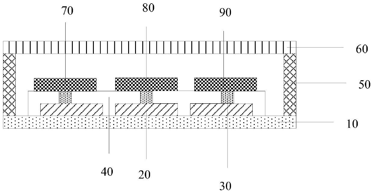
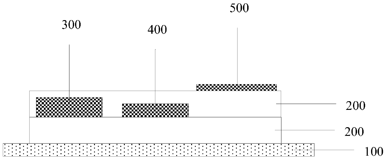
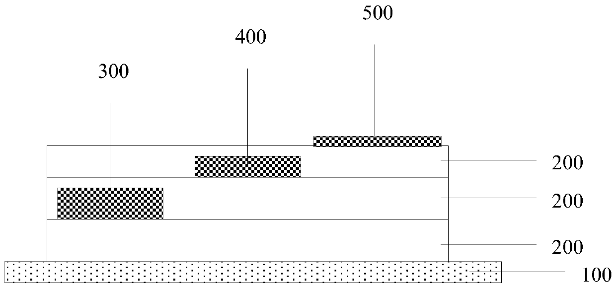
[0032] The embodiment of the present application provides an organic light emitting display panel, refer to figure 2 and image 3 , figure 2 and image 3 It is a schematic cross-sectional structure diagram of the organic light emitting display panel, and the organic light emitting display panel includes:

[0033] the first substrate 100;

[0034] At least two pixel definition layers 200 located on one side surface of the first substrate 100, the pixel de...


PUM


Abstract

The application discloses a display device, an organic light emitting display panel and a manufacturing method thereof. Wherein, the organic light-emitting display panel includes: a first substrate; at least two pixel definition layers located on one side surface of the first substrate, and the pixel definition layers are insulated from each other; multiple pixels located on the surfaces of the at least two pixel definition layers a display pixel, the display pixel includes a first sub-pixel, a second sub-pixel and a third sub-pixel, wherein at least two of the first sub-pixel, the second sub-pixel and the third sub-pixel are located in different Pixels define the layer surface. The organic light-emitting display panel reduces the possibility of signal crosstalk caused by signal coupling when adjacent sub-pixels receive display signals during the display process; and improves the display due to the increase in the distance between adjacent sub-pixels The pixel design space increases the designable width of the wiring between the display pixel and the pixel driving film layer of the organic light emitting display panel.

Description

technical field [0001] The present application relates to the field of display technology, and more specifically, to a display device, an organic light-emitting display panel and a manufacturing method thereof. Background technique [0002] With the continuous development of display technology, the application of display panels is becoming more and more extensive. Organic Light Emitting Diode (OLED) display panels have become a rising star in the display panel industry due to their advantages such as fast response speed, brilliant colors, thinness and convenience. [0003] refer to figure 1 , figure 1 It is a schematic cross-sectional structure diagram of an organic light-emitting display panel in the prior art, specifically including: a substrate 10, a pixel driving circuit 20 located on the surface of the substrate 10, and a pixel definition layer 40, the pixel definition layer 40 has a plurality of connection through holes 30, A plurality of display pixels located on th...

Claims


Application Information

Patent Timeline
Patent Type & Authority Patents(China)
IPC IPC(8): H01L27/32H01L51/56
CPCH10K59/35H10K71/00
Inventor 刘丽媛熊志勇胡天庆
Owner WUHAN TIANMA MICRO ELECTRONICS CO LTD
Features
  • R&D
  • Intellectual Property
  • Life Sciences
  • Materials
  • Tech Scout
  • Unparalleled Data Quality
  • Higher Quality Content
  • 60% Fewer Hallucinations
Learn More