Circuit board structure, packaging structure and method for making the same

a technology of circuit board and packaging, applied in the manufacture of printed circuits, basic electric elements, solid-state devices, etc., can solve the problem of not being able to provide more pins, and achieve the effect of reducing packaging size, facilitating the release of carrier and copper film, and increasing design spa

Inactive Publication Date: 2011-10-27
ADVANCE MATERIALS CORP
View PDF3 Cites 1 Cited by
  • Summary
  • Abstract
  • Description
  • Claims
  • Application Information

AI Technical Summary

Benefits of technology

[0011]The present invention hence proposes a novel circuit board structure, a package structure and the fabrication methods thereof. The circuit board structure and the package structure of the present invention employ an area array design to decrease the packaging size by increasing the design space. Besides, the release film of the present invention facilitates the release of the carrier and the copper film.

Problems solved by technology

However, as the data processed by the die increases and the speed for processing needs to be higher, the lead frame as illustrated cannot provide more pins 120 to meet the demands because the space around the die is so limited.

Method used


Image

  • Circuit board structure, packaging structure and method for making the same
  • Circuit board structure, packaging structure and method for making the same
  • Circuit board structure, packaging structure and method for making the same

Examples


Embodiment Construction

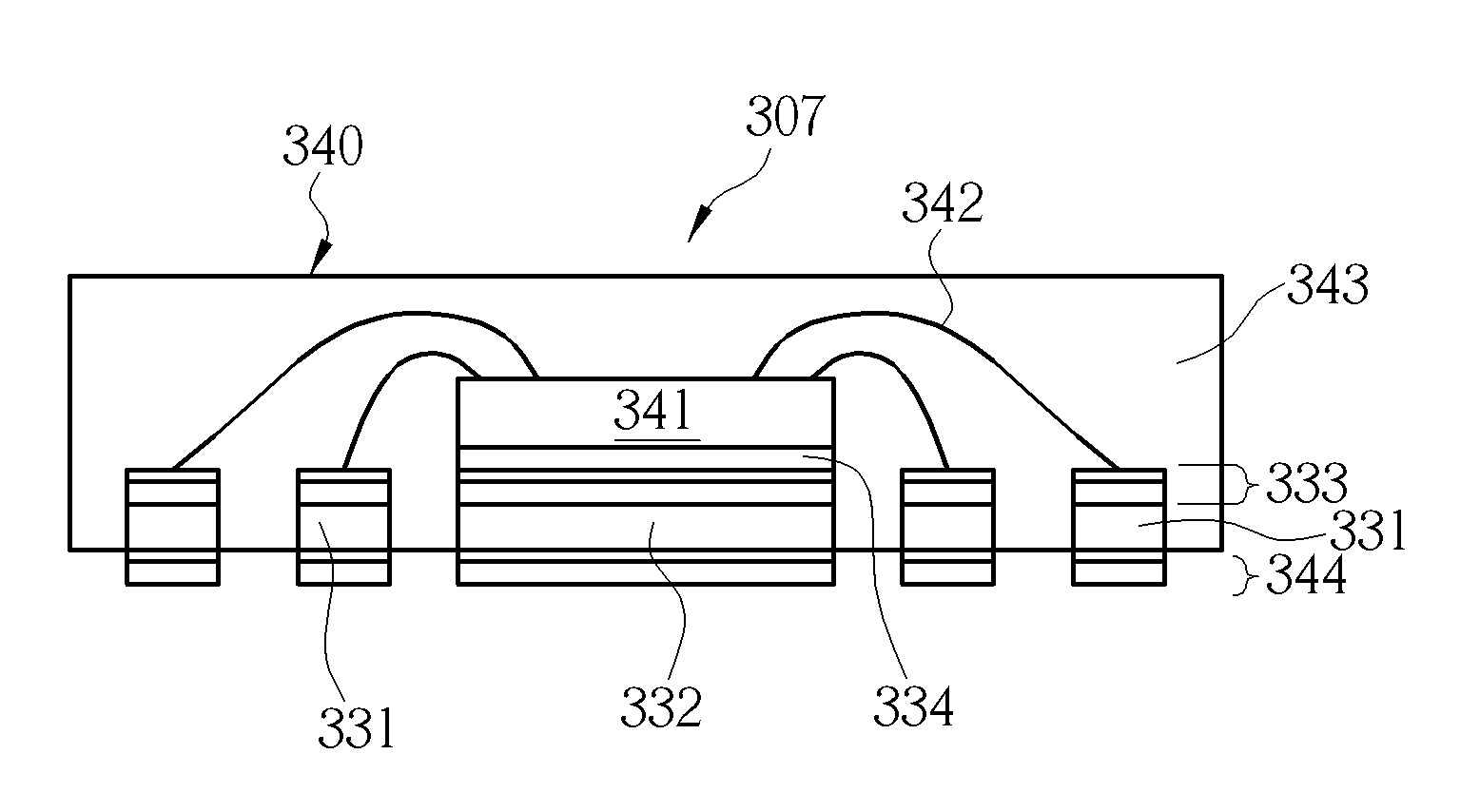
[0027]The present invention in a first aspect provides a method for making a circuit board structure. FIGS. 7-8 illustrate the method for making a circuit board structure of the present invention. Please refer to FIG. 7, first a substrate 309 is provided. The substrate 309 includes a carrier 310, a release film 320 and a copper film 330. The release film 320 is disposed between the carrier 310 and the copper film 330. The carrier 310 may be any suitable material, such as polyethylene terephthalate (PET), polycarbonate (PC), polymethylmethacrylate (PMMA) or a copperless substrate. The release film 320 may be a plastic and sticky material and has better adhesion to the carrier 310. The release film 320 accordingly adheres to one side of the carrier 310 by means of the adhesion. The substrate 309 may have a thickness of about 150 μm-400 μm, preferably 265 μm.

[0028]The carrier 310, the release film 320 and the copper film 330 in the substrate 309 may optionally have different processing...


PUM


Abstract

A method for making a circuit board structure is disclosed. First, a substrate is provided. The substrate includes a carrier, a copper film and a release film disposed between them. Next, the copper film is patterned to form a connecting pattern and a die pad. Later, a passivation layer is formed to cover the connecting pattern and the die pad.

Description

BACKGROUND OF THE INVENTION[0001]1. Field of the Invention[0002]The present invention generally relates to a method for making a circuit board structure, the circuit board structure and the package structure obtained therefrom. In particular, the present invention is directed to a method for making a circuit board structure and a package structure by means of a carrier and a copper film with a release film attached thereon.[0003]2. Description of the Prior Art[0004]A circuit board is an essential component of an electronic device. With the trend of always scaling down the size of the electronic devices, various carrier structures are therefore proposed to support the die. Some pins extend outwards to connect other circuits surrounding the circuit board to form proper electrical connections.[0005]As far as the current technology is concerned, a circuit structure called “lead frame” is conventionally known. FIGS. 1-4 illustrate a method for making a traditional lead frame. Please refe...

Claims


Application Information

Patent Timeline
Patent Type & Authority Applications(United States)
IPC IPC(8): H01L23/48H01L21/56H05K1/11
CPCH01L23/3121H01L23/49582H01L2924/01028H01L2224/29339H01L2924/014H01L2924/01033H01L2924/01006H05K3/20H05K3/06H01L2924/15311H01L2924/01082H01L2924/01079H01L2924/0105H01L2924/01047H01L2924/01029H01L2224/85455H01L2224/85444H01L2224/85439H01L2224/73265H01L2224/48247H01L2224/48227H01L2224/48091H01L2224/45644H01L2224/45565H01L2224/45147H01L24/29H01L24/32H01L24/45H01L24/48H01L24/85H01L2224/29099H01L2224/32245H01L2224/45139H01L2224/45144H01L2924/00014H01L2924/00012H01L2224/48639H01L2224/48839H01L2224/48844H01L2224/48855H01L2224/48644H01L2224/48655H01L24/73H01L2924/181H01L2924/00H01L2224/45015H01L2924/207
Inventor YEN, LEE-SHENG
Owner ADVANCE MATERIALS CORP
Why Eureka
Try Eureka