Flipchip QFN package and method therefor

a technology of integrated circuits and flipchips, applied in the direction of semiconductor devices, semiconductor/solid-state device details, electrical apparatus, etc., can solve the problems of continuous pressure on the need for small, yet less expensive packaged ics, size and cost of electronic devices

Active Publication Date: 2005-03-15
NORTH STAR INNOVATIONS
View PDF12 Cites 42 Cited by
  • Summary
  • Abstract
  • Description
  • Claims
  • Application Information

AI Technical Summary

Benefits of technology

Use of packaged ICs is widespread. Móreover, the size and cost of electronic devices puts continuous pressure on the need for small, yet less costly packaged ICs. Furthermore, for high bandwidth RF devices and high operating frequency devices, there is a push for shorter electrical paths inside the IC package. Flip chip bonding can replace the traditional wire bonding interconnection. Thus, it is desirable to provide an inexpensive method of flip chip interconnection packaging ICs. It also is desirable to have a method of decreasing the size of such packaged ICs.

Problems solved by technology

Móreover, the size and cost of electronic devices puts continuous pressure on the need for small, yet less costly packaged ICs.

Method used


Image

  • Flipchip QFN package and method therefor
  • Flipchip QFN package and method therefor
  • Flipchip QFN package and method therefor

Examples


Embodiment Construction

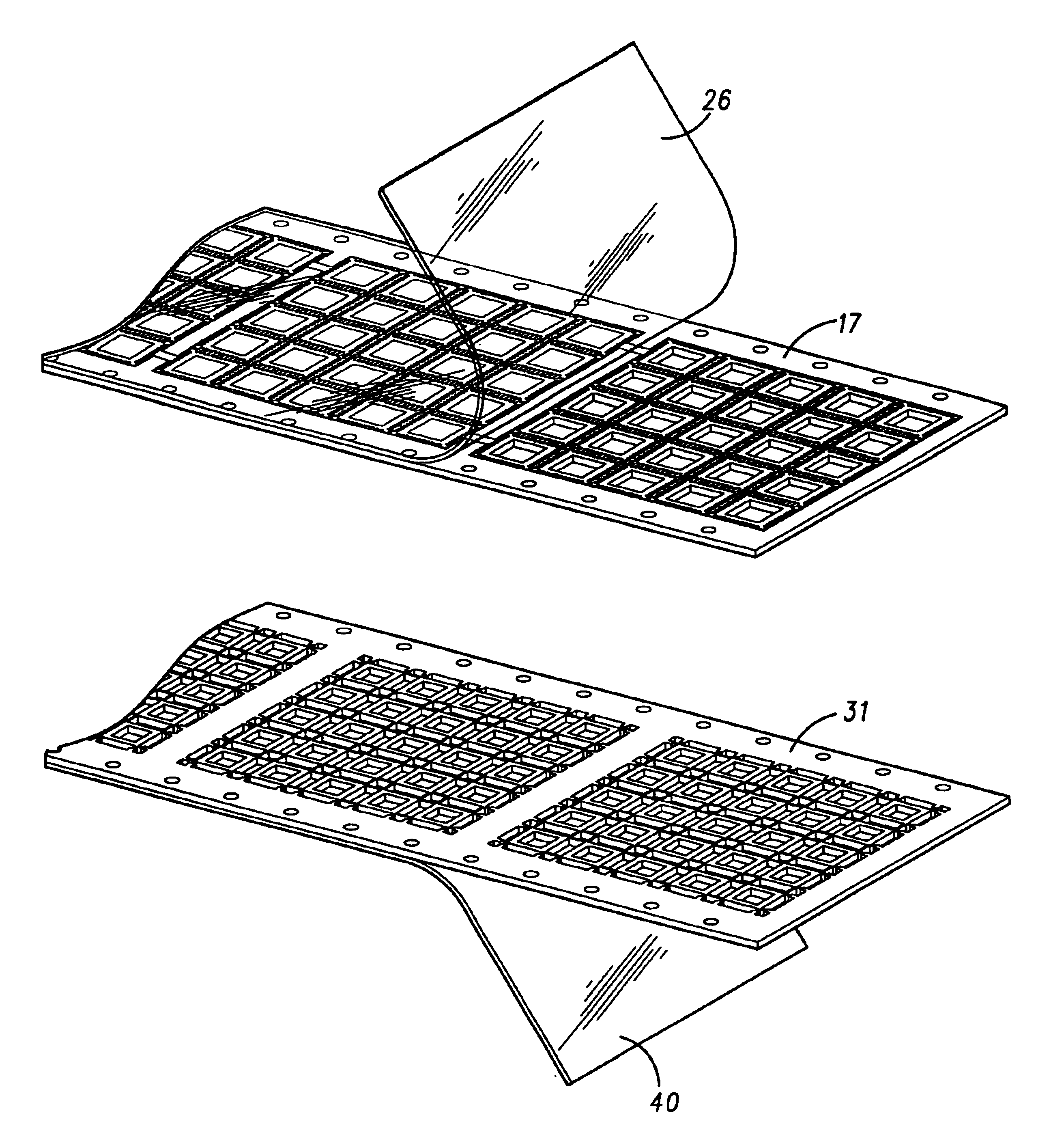
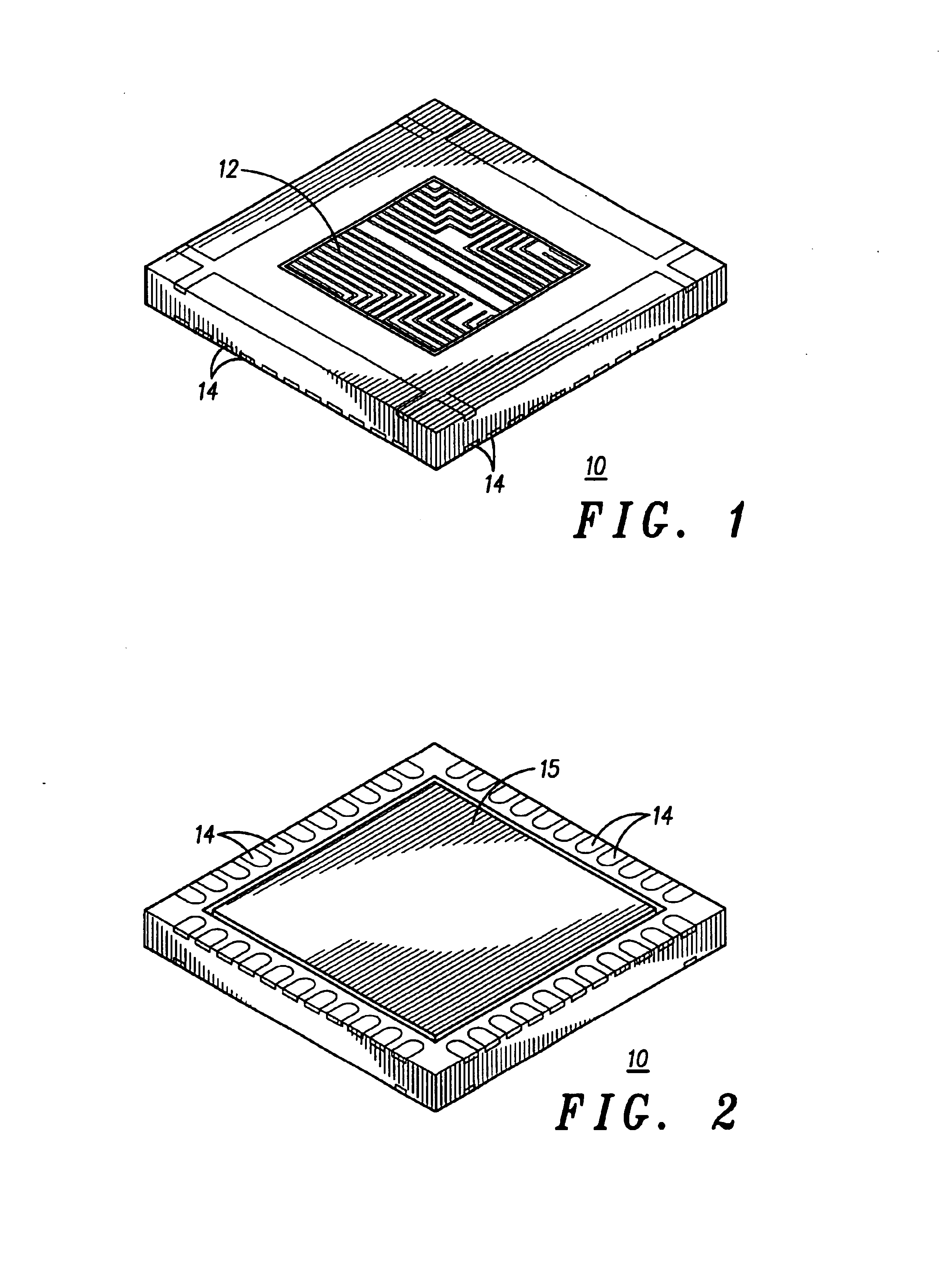
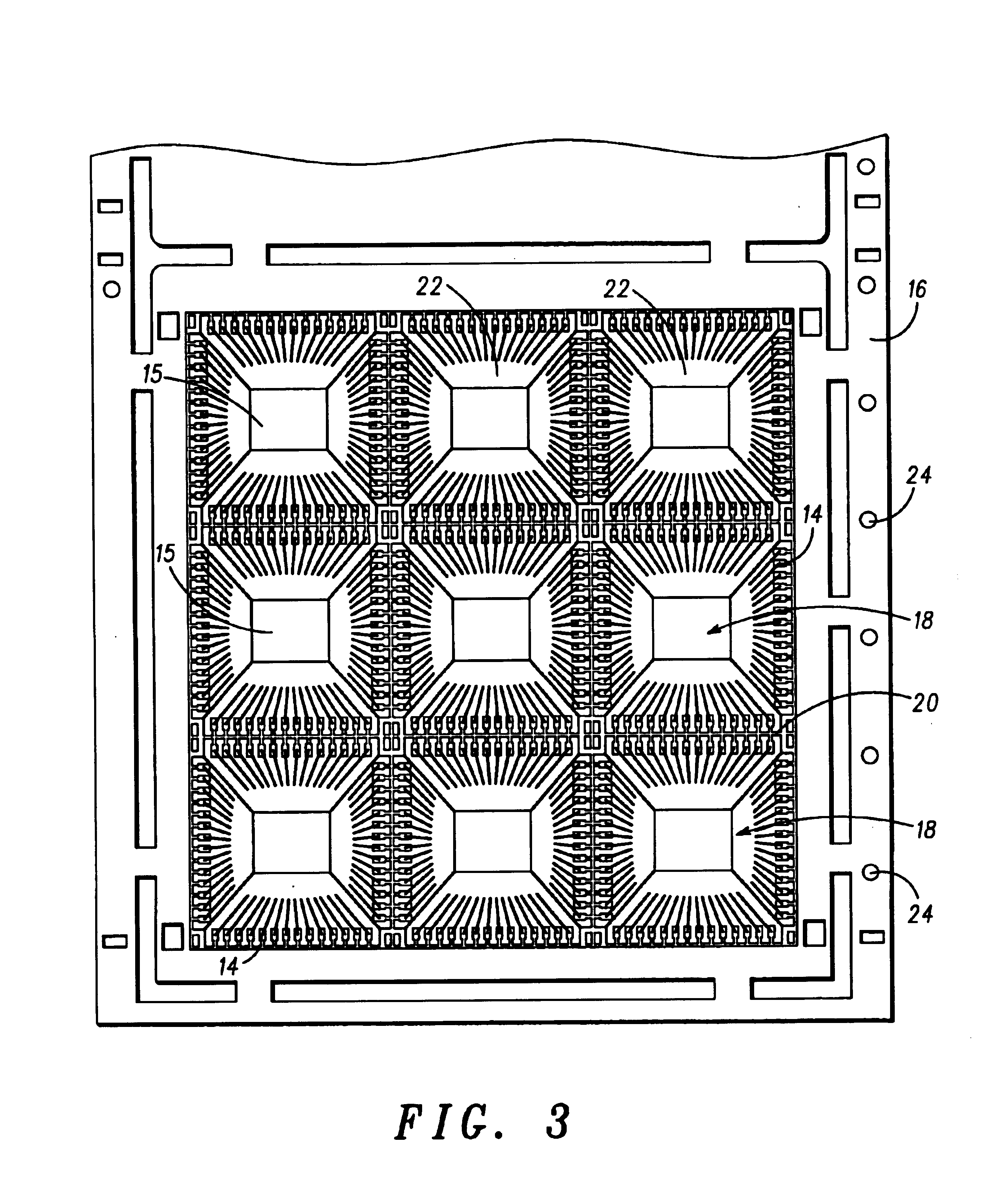
The detailed description set forth below in connection with the appended drawings is intended as a description of the presently preferred embodiment of the invention, and is not intended to represent the only form in which the present invention may be practiced. It is to be understood that the same or equivalent functions may be accomplished by different embodiments that are intended to be encompassed within the spirit and scope of the invention. As will be understood by those of skill in the art, the present invention can be applied to various packages and package types.

Certain features in the drawings have been enlarged for ease of illustration and the drawings and the elements thereof are not necessarily in proper proportion. Further, the invention is shown embodied in a Quad Flat No-lead (QFN) type package. However, those of ordinary skill in the art will readily understand the details of the invention and that the invention is applicable to other package types. In the drawings,...


PUM


Abstract

A semiconductor device (10) includes a first leadframe (18) having a perimeter (20) that defines a cavity (22) and leads (14) extending inwardly from the perimeter, and a second leadframe (32) having top and bottom surfaces and a die paddle surrounding a die receiving area (36). An integrated circuit (12) is placed within the die receiving area of the second leadframe. The IC has bonding pads (44) located on a peripheral portion of its top surface. The second leadframe and the IC are in facing relation with the first leadframe such that the leads of the first leadframe are electrically connected to respective ones of the bonding pads. A mold compound (50) is injected between the first and second leadframes and covers the second leadframe top surface and a central area of the first surface of the IC. At least the bottom surfaces of the leads are exposed.

Description

BACKGROUND OF THE INVENTIONThe present invention relates to integrated circuits and packaged integrated circuits and, more particularly, to a packaged integrated circuit formed using two separate leadframes.An integrated circuit (IC) die is a small device formed on a semiconductor wafer, such as a silicon wafer. A leadframe is a metal frame that usually includes a paddle that supports an IC die that has been cut from the wafer. The leadframe has lead fingers that provide external electrical connections. That is, the die is attached to the die paddle and then bonding pads of the die are connected to the lead fingers via wire bonding or flip chip bumping to provide the external electrical connections. Encapsulating the die and wire bonds or flip chip bump with a protective material forms a package. Depending on the package type, the external electrical connections may be used as-is, such as in a Thin Small Outline Package (TSOP), or further processed, such as by attaching spherical so...

Claims


Application Information

Patent Timeline
Patent Type & Authority Patents(United States)
IPC IPC(8): H01L21/56H01L23/495H01L23/31H01L21/02H01L23/28H01L23/48
CPCH01L21/566H01L23/4952H01L23/49537H01L23/49548H01L24/97H01L23/3107H01L2924/18161H01L2224/97H01L2924/01015H01L2924/01029H01L2924/01033H01L2924/01078H01L2924/01079H01L2924/01082H01L2924/14H01L2224/81001H01L2924/01005H01L2924/01006H01L2224/16245H01L2224/81H01L2924/181H01L2224/05573H01L2224/05568H01L2924/00014H01L2924/00H01L2224/05599H01L23/495H01L23/02
Inventor SHIU, HEI MINGCHOW, WAI WONGHE, QING-CHUN
Owner NORTH STAR INNOVATIONS
Why Eureka
Try Eureka