Efficient welding method for semiconductor packaging

A welding method and semiconductor technology, applied in the direction of semiconductor devices, semiconductor/solid-state device manufacturing, electric solid-state devices, etc., can solve the first welding wire welding spot and arc damage, affect the second welding wire welding and arcing, reduce Ultrasonic bonding operation efficiency and other issues, to achieve the effect of high wire bonding operation efficiency, efficiency improvement, and high conduction current

Inactive Publication Date: 2020-04-24
常州市润祥电子科技有限公司
View PDF3 Cites 2 Cited by
  • Summary
  • Abstract
  • Description
  • Claims
  • Application Information

AI Technical Summary

Problems solved by technology

[0004] The traditional ultrasonic bonding process adopts the welding method of single welding single welding wire, so that a single product needs multiple ultrasonic welding to complete the repeated welding of two or more welding wires on a single product, which will reduce the ultrasonic bonding operation. At the same time, limited by the structural characteristics of the rivet and the wire conduit, after the first welding wire is welded, if the distance between the welding point position of the second welding wire and the welding point position of the first welding wire is too narrow, the rivet or The wire tube will touch the welding spot or arc of the first welding wire, which will not only affect the welding and arc drawing of the second welding wire, but also cause damage to the welding spot and arc of the first welding wire, so two or more A certain spacing and space need to be reserved in the process of root wire welding and arc formation, which brings certain process restrictions to chip structure design and packaging design.

Method used


Image

  • Efficient welding method for semiconductor packaging
  • Efficient welding method for semiconductor packaging
  • Efficient welding method for semiconductor packaging

Examples


Embodiment Construction

[0040] The technical solutions in the embodiments of the present invention will be clearly and completely described below in conjunction with the accompanying drawings in the embodiments of the present invention. Obviously, the described embodiments are only a part of the embodiments of the present invention, rather than all the embodiments. Based on the embodiments of the present invention, all other embodiments obtained by those of ordinary skill in the art without creative work shall fall within the protection scope of the present invention.

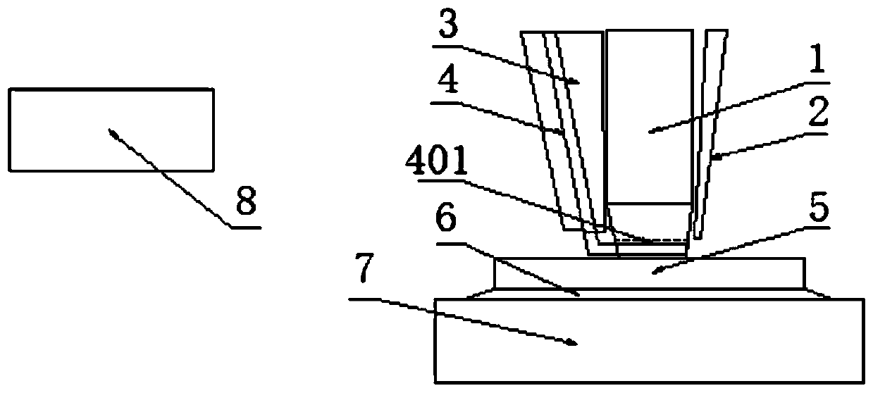
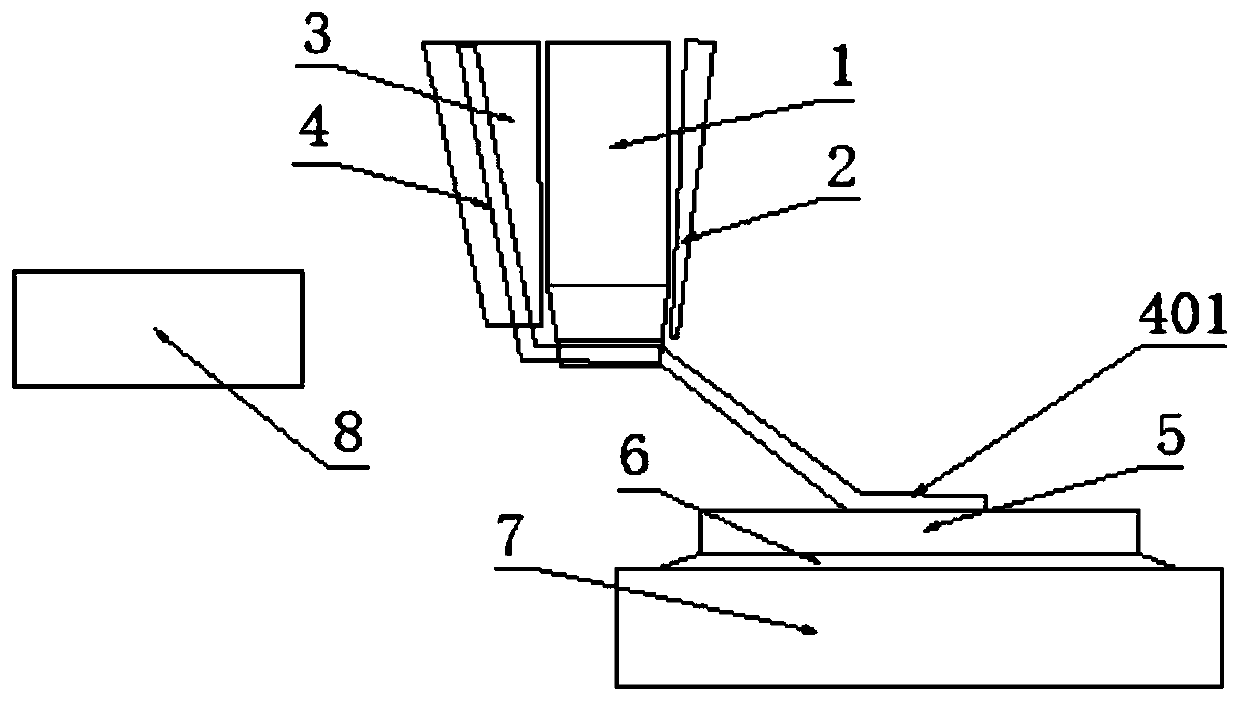
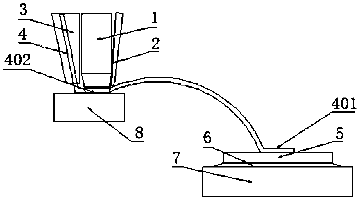
[0041] See attached Figure 1-9 As shown, this embodiment is an efficient soldering method for semiconductor packaging, which includes the following steps:

[0042] Step 1: According to the number of welding wires of the product, select the matching multi-purpose spool 9, multi-hole threading tube, multi-head conduit 3 and multi-wire slot wedge 1. The number of welding wires 4 is at least two, and each wire is 4 The wire diameters are the...


PUM


Abstract

The invention belongs to the technical field of semiconductor packaging, and particularly relates to an efficient welding method for semiconductor packaging. The efficient welding method comprises thesteps of according to the number of welding wires of a product, selecting a multi-purpose spool, a multi-hole threading pipe, a multi-head wire conduit and a multi-welding-wire-groove chopper which match one another; carrying out multi-purpose spool fixing and welding wire conveying; welding a welding wire on the chip; forming a line arc; and carrying out frame pin welding. By means of the welding method, multiple welding wires can be welded to a single product at a time, and the wire welding operation efficiency is improved extremely efficiently. By means of the welding method, when multiplewelding wires are welded at a time, gaps and spaces reserved in a traditional welding mode can be avoided, and higher design space is brought to the design of a chip pressure area. The original chippressure area can contain the welding wires with the larger wire diameter, and the requirement for higher breakover current is met.

Description

Technical field [0001] The invention belongs to the technical field of semiconductor packaging, and specifically relates to an efficient welding method for semiconductor packaging. Background technique [0002] The welding wire of the ultrasonic bonding process at room temperature can be welded with aluminum wire, aluminum strip, copper wire or other alloy materials. Because these materials have good performance and strength, they are more and more widely used in power device packaging in recent years. With the continuous development of society, power semiconductor devices capable of carrying higher power have been widely used in the fields of telecommunication server power supply, induction heating applications, uninterruptible power supplies, mobile phones, automotive electronics, plasma TVs, LCD TVs and other fields. With the development of power devices in the direction of high power, high frequency, and integration, terminal products have higher and higher requirements for c...

Claims


Application Information

Patent Timeline
Patent Type & Authority Applications(China)
IPC IPC(8): H01L21/60
CPCH01L24/85H01L2224/85205H01L2224/92247H01L2224/85181H01L2224/48472H01L2224/32245H01L2224/49111H01L2224/73265H01L2224/78H01L2224/78313H01L2224/48247H01L2924/00
Inventor 赵伟丹
Owner 常州市润祥电子科技有限公司
Why Eureka
Try Eureka