Touch substrate and manufacturing method thereof and touch device
A substrate and touch technology, applied in the direction of instruments, electrical digital data processing, data processing input/output process, etc., can solve the unfavorable narrow frame design of touch display devices, large wiring area width, and insufficient signal line width Further reduction and other issues
- Summary
- Abstract
- Description
- Claims
- Application Information
AI Technical Summary
Problems solved by technology
Method used
Image
Examples
Embodiment 1
[0050] Such as Figure 4 As shown, the first touch electrode 101 in the touch substrate 10 has an integrated structure, and the second touch electrode 102 includes a row of touch sub-electrodes 1020 and bridge point patterns 1022 connecting adjacent touch sub-electrodes 1020. The sub-electrodes 1020 are disposed on the same layer as the first touch electrodes 101 , and the bridge point patterns 1022 are disposed on different layers from the first touch electrodes 101 .
[0051] The specific arrangement of the second signal line 12 will be described below.
[0052] For example, the second signal line 12 can be arranged on the same layer as the bridge point pattern 1022, and the bridge point pattern 1022 and the second signal line 12 are made of metal material. The second signal line 12 can simplify the manufacturing process and reduce the manufacturing cost.
[0053] For another example, the second signal line 12 and the bridge point pattern 1022 can be arranged on the same l...
Embodiment 2
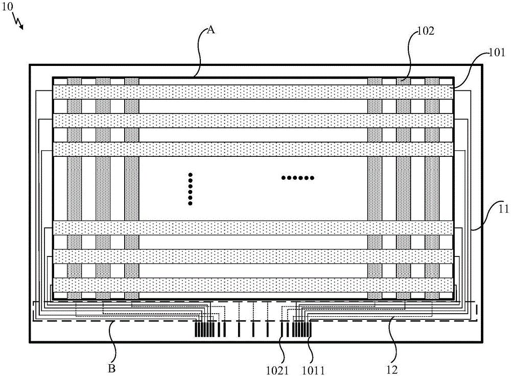
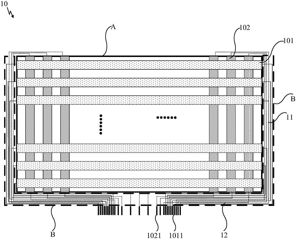
[0064] Such as figure 2 As shown in or 3, the first touch electrode 101 and the second touch electrode 102 are all integral structures.
[0065] In this case, the first signal line 11 and the first touch electrode 101 are arranged on the same layer, that is, both the first signal line 11 and the first touch electrode 101 are made of transparent conductive material, and the second signal line 12 and the second touch electrode The electrodes 102 are arranged in different layers, and the second signal line 12 is made of metal material. Alternatively, the second signal line 12 and the second touch electrode 101 are arranged on the same layer, that is, both the second signal line 12 and the second touch electrode 101 are made of transparent conductive material, and the first signal line 11 is different from the first touch electrode 101. Layers are provided, and the first signal line 11 is made of metal material.
[0066] By making the signal line arranged on the same layer as t...
PUM
 Abstract
Description
Claims
Application Information


