Pixel structure

A pixel structure and pixel area technology, applied in nonlinear optics, instruments, optics, etc., can solve the problems of electric field changes and curved surface display darkening, and achieve the effect of reducing dark lines and improving display quality

Inactive Publication Date: 2017-03-22
AU OPTRONICS CORP
View PDF0 Cites 9 Cited by
  • Summary
  • Abstract
  • Description
  • Claims
  • Application Information

AI Technical Summary

Problems solved by technology

[0006] In the process of making a curved display, since the upper and lower substrates are based on the center of the panel, there will be a relative shift (shift) to the left and right sides in the horizontal direction, which will cause a relative shift of the ITO Trunk in the thin film transistor array substrate, and the pixel The electric field in the cell will change, causing the position near the ITO Trunk in the curved display to be dark

Method used


Image

  • Pixel structure
  • Pixel structure
  • Pixel structure

Examples


Embodiment Construction

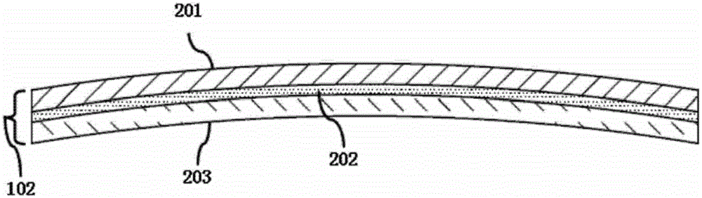
[0037] refer to figure 1 , figure 1 Schematic cross-section of a curved display panel. The curved display panel 102 of this embodiment includes a curved color filter substrate 201 , a liquid crystal layer 202 and a thin film transistor array substrate 203 .

[0038] Wherein, the curved color filter substrate 201 includes components such as a curved substrate, a color-resistor array layer, and a common electrode, which can be changed according to design requirements, and the present invention is not limited thereto.

[0039] The curved TFT array substrate 203 includes a curved substrate, a pixel array layer and a protective layer. The pixel array layer includes scan line arrays, data line arrays, thin film transistor switch arrays, pixel electrode arrays and other components, which can be changed depending on the needs of the design, and the present invention is not limited thereto. The curved color filter substrate 203 and the curved thin film transistor array substrate 201...


PUM


Abstract

The invention discloses a pixel structure. The pixel structure comprises a substrate provided with a pixel zone, a pixel electrode located in the pixel zone, multiple branch electrodes and shielding parts located below the pixel electrode, wherein the pixel electrode comprises a main electrode extending in the first direction of the pixel zone and the second direction perpendicular to the first direction, the multiple branch electrodes extend from the main electrode to the edge of the pixel zone, a slit is formed between every two adjacent branch electrodes, and the shielding parts include a first shielding part extending only along the main electrode in the second direction, only covering the main electrode in the second direction and corresponding to the main electrode in arrangement and a second shielding part outwards extending only along the first shielding part, only covering the slits and corresponding to the slits in arrangement. Dark fringes produced in juncture areas of different zones in the pixel electrode can be decreased by adopting the pixel structure, and accordingly the display quality is improved.

Description

technical field [0001] The present invention relates to a pixel structure, especially a pixel structure with a vertically oriented display device. Background technique [0002] In recent years, thin and light liquid crystal display devices are being used as display devices used in monitors of personal computers or display portions of portable information terminal devices. However, the existing TN (Twisted Nematic: twisted nematic) type or STN (Super Twisted Nematic: super twisted nematic) type liquid crystal display device has the disadvantage of a narrow viewing angle. In order to solve this problem, various technologies are being carried out. develop. [0003] An alignment split type liquid crystal display device including a vertical alignment type liquid crystal layer is known as a liquid crystal display device having improved viewing angle characteristics. Such a liquid crystal display device is called a VA (Vertical Alignment) mode liquid crystal display device. MVA ...

Claims


Application Information

Patent Timeline
Patent Type & Authority Applications(China)
IPC IPC(8): G02F1/1343G02F1/139
CPCG02F1/134309G02F1/139
Inventor 张乃文何昇儒陈宜瑢
Owner AU OPTRONICS CORP
Why Eureka
Try Eureka