Double-surface display device
A double-sided display device and encapsulation layer technology, which is applied to electrical components, electrical solid-state devices, circuits, etc., can solve the problems of complex TFT structure, low panel utilization rate, and complicated process procedures, and achieve the effect of improving area utilization rate.
- Summary
- Abstract
- Description
- Claims
- Application Information
AI Technical Summary
Problems solved by technology
Method used
Image
Examples
Embodiment Construction
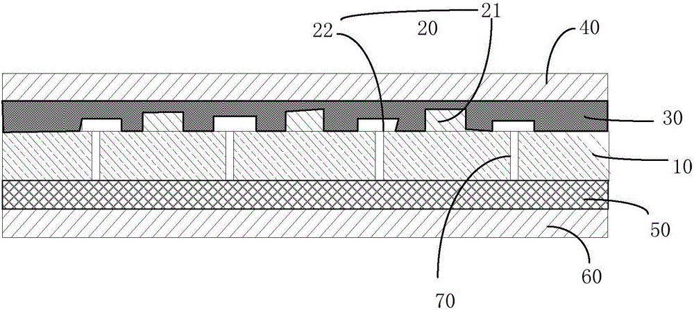
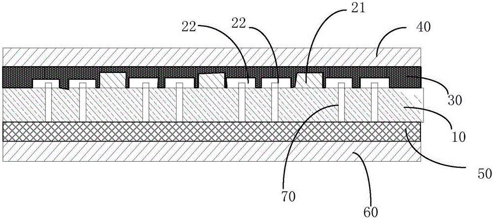
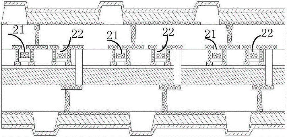
[0031] see Figure 1a and Figure 1b and Figure 2a and Figure 2b , is a schematic structural view of the first embodiment of the double-sided display device of the present invention. The double-sided display device includes a substrate 10, a TFT layer 20, a first light-emitting layer 30, and a first encapsulation layer 40 stacked in sequence above the substrate 10, and a second light-emitting layer stacked in sequence below the substrate 10. 50 and the second encapsulation layer 60 , wherein a plurality of via holes 70 penetrate through the substrate 10 and electrically connect the TFT layer 20 with the first light emitting layer 30 and the second light emitting layer 50 . Wherein, the first and second luminescent layers both include an anode, a luminescent material layer and a cathode. Although the present invention simplifies the double-sided display device into four structures of substrate, TFT layer, light-emitting layer, and encapsulation layer, these four structures...
PUM
 Abstract
Description
Claims
Application Information


