Buck-boost conversion device

A technology of buck-boost conversion and voltage sampling, which is applied in the electronic field, can solve the problems of design difficulty, waste of resources and cost, and achieve the effect of reducing operation difficulty and cost

Pending Publication Date: 2017-04-26
CHIPONE TECH BEIJINGCO LTD
View PDF4 Cites 8 Cited by
  • Summary
  • Abstract
  • Description
  • Claims
  • Application Information

AI Technical Summary

Problems solved by technology

As mentioned above, since the pulse control signals used to control the main circuit are different in different modes, two different control circuits are currently required to control the main circuit in the two modes, which not only brings design problems to designers and operational difficulty, but also a waste of resources and costs

Method used


Image

  • Buck-boost conversion device
  • Buck-boost conversion device
  • Buck-boost conversion device

Examples


Embodiment Construction

[0030] Hereinafter, the present invention will be described in more detail with reference to the accompanying drawings. In the various figures, identical elements are indicated with similar reference numerals. For the sake of clarity, various parts in the drawings have not been drawn to scale. Also, some well-known parts may not be shown in the drawings.

[0031] In the following, many specific details of the present invention are described, such as device structures, materials, dimensions, processing techniques and techniques, for a clearer understanding of the present invention. However, the invention may be practiced without these specific details, as will be understood by those skilled in the art.

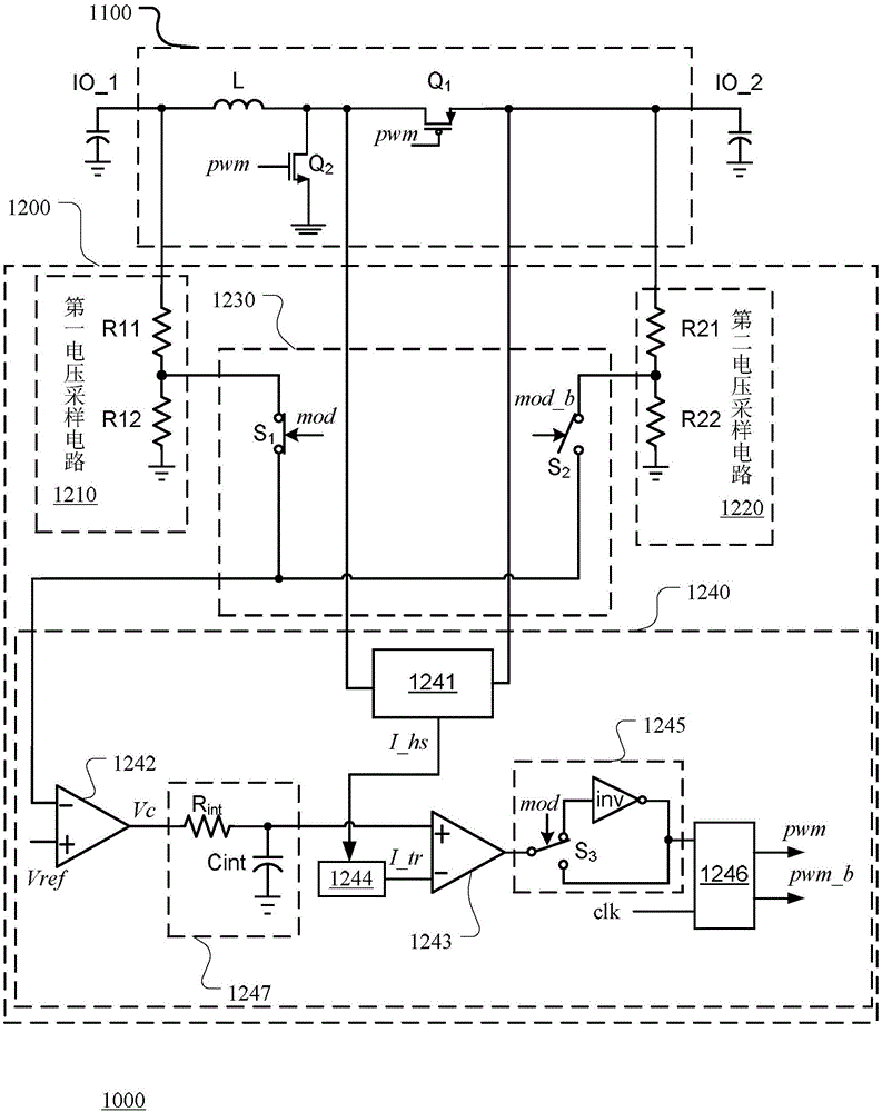
[0032] image 3 A schematic structural diagram of a buck-boost conversion device according to an embodiment of the present invention is shown.

[0033] like image 3 As shown, the buck-boost conversion device 1000 of the embodiment of the present invention includes a main ...


PUM


Abstract

The invention provides a buck-boost conversion device. The device comprises a main circuit and a control circuit, wherein the main circuit possesses a first port and a second port; the main circuit is used for converting an input voltage received by one of the first port and the second port according to a pulse control signal into an output voltage and the output voltage is output by another one of the first port and the second port; the control circuit is used for providing the pulse control signal; the control circuit generates an adjusting signal according to a feedback signal of the output voltage; under a boost mode, according to the adjusting signal, the pulse control signal is generated; and under a buck mode, according to an anti-phase signal of the adjusting signal, the pulse control signal is generated. By using the buck-boost conversion device in an embodiment, based on a condition of guaranteeing performance and a function, a uniform circuit are used to control boost and buck modes of a main circuit in the buck-boost conversion device; and a designer can conveniently carry out boost and buck function conversion on the circuit so that operation difficulty, and a circuit area and cost are reduced.

Description

technical field [0001] The present invention relates to the field of electronic technology, and more specifically, to a buck-boost conversion device. Background technique [0002] At present, in the switching power supply circuit, the main circuit is mainly implemented by two architectures: Buck architecture and Boost architecture, each architecture includes two transistors that play the role of switching and freewheeling respectively. Among them, the Buck architecture is used to reduce the input voltage, and the Boost architecture is used to reduce the input voltage. These two structures are usually implemented by different types of chips. [0003] To save resources, such as figure 1 and figure 2 As shown, a prior art utilizes a unified main circuit 100 to implement two architectures. [0004] like figure 1 As shown, when the main circuit 100 works in the step-down mode, the second port IO_2 of the main circuit receives the input voltage Vin provided by the input power...

Claims


Application Information

Patent Timeline
Patent Type & Authority Applications(China)
IPC IPC(8): H02M3/158
CPCH02M3/1582
Inventor 李东金宁
Owner CHIPONE TECH BEIJINGCO LTD
Why Eureka
Try Eureka