High-speed 3D electrical characteristic test system applied to transistors

A technology of electrical characteristics and testing system, which is applied in the direction of single semiconductor device testing, measuring electricity, measuring devices, etc., and can solve problems such as inability to fully reflect the transport movement of carriers and defects

Active Publication Date: 2017-05-10
ZHEJIANG UNIV
View PDF6 Cites 7 Cited by
  • Summary
  • Abstract
  • Description
  • Claims
  • Application Information

AI Technical Summary

Problems solved by technology

The fastest Rapid I currently reported DS -V GS In the test method, the rising and falling edges are a few nanoseconds, which cannot fully reflect the transport movement between carriers and defects

Method used


Image

  • High-speed 3D electrical characteristic test system applied to transistors
  • High-speed 3D electrical characteristic test system applied to transistors
  • High-speed 3D electrical characteristic test system applied to transistors

Examples


Embodiment Construction

[0019] The technical solution of the present invention will be described in detail below in conjunction with the accompanying drawings and specific embodiments.

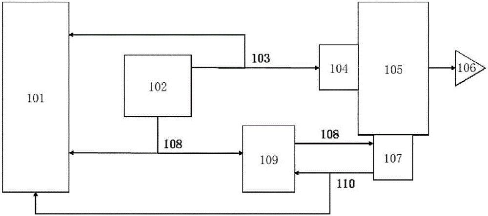
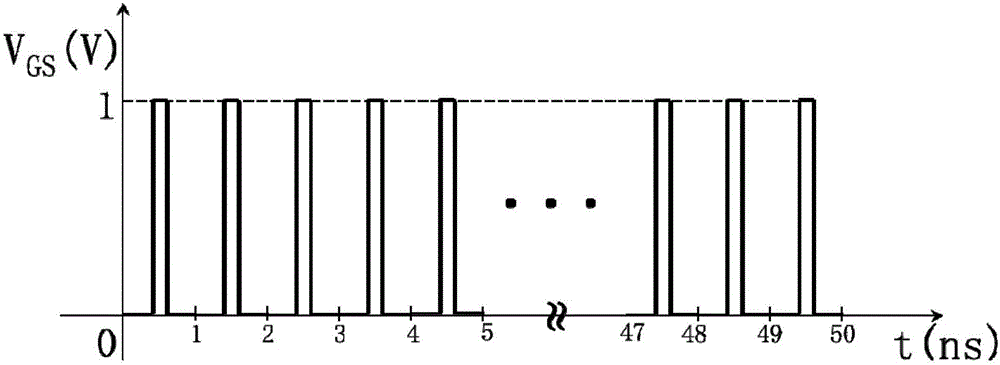
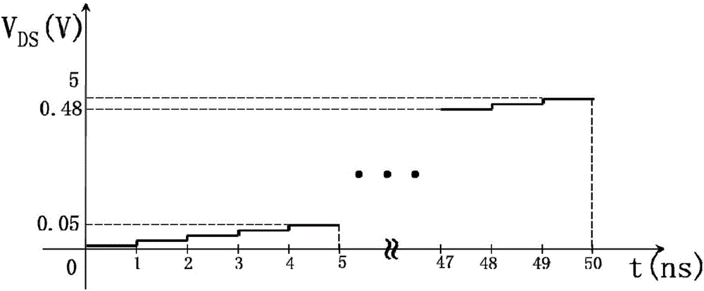
[0020] Such as figure 1 As shown, a high-speed three-dimensional electrical characteristic testing system applied to transistors, the system includes a data feedback and processor 101, a waveform processor 102, a broadband pick-up tee device 109, a first microwave probe 104 and a second microwave Probe 107. The first channel of the waveform processor 102 generates a pulse voltage waveform whose rising edge and falling edge are less than 100 pS as the gate voltage signal 103, which is loaded on the gate of the MOSFET transistor 105 to be tested by the first microwave probe 104; the waveform processor The second channel of 102 generates a stepped voltage waveform as a drain voltage signal 108, and loads the drain voltage signal 108 on the drain of the MOSFET transistor 105 to be tested; while ensuring the integrity of...


PUM


Abstract

The invention discloses a high-speed 3D electrical characteristic test system applied to transistors. The system comprises a data feedback and processor, a waveform processor, a broadband pick-up three-way device, a first microwave probe, and a second microwave probe. The innovation of the system is that a transistor transfer characteristics test is conducted by applying a gradient voltage waveform to the drain of a transistor and applying a pulse voltage signal to the gate of the transistor in each stepped level, and the 3D electrical characteristic (IDS-VGS-VDS), transfer characteristic (IDS-VGS) and output characteristic (IDS-VDS) of the transistor are tested in 100ns. The system is applied to the electrical characteristic research of a high-performance planar transistor using silicon, germanium or an III-V-group compound as a carrier sub-channel and a fin type three-dimensional gate-structure or GAA-structure metal oxide semiconductor field effect transistor.

Description

technical field [0001] The invention belongs to the technical field of metal oxide semiconductor field effect transistor electrical characteristic testing and parameter extraction, and specifically relates to an electrical test for a high-performance transistor device within a very short time (1nS), and the three-dimensional measurement of the transistor within 100nS Electrical characteristics (I D -V GS -V DS ), transfer characteristics (I DS -V GS ) and output characteristics (I DS -V DS ) high-speed test system. Background technique [0002] Semiconductor technology continues to develop in accordance with Moore's Law, the integration of integrated circuits doubles every two years, and the characteristic gate length of Metal Oxide Semiconductor Field Effect Transistor (MOSFET) continues to shrink, from micron to sub-micron to the present 14nm technology. While the characteristic gate length of MOSFET is continuously shrinking, in order to continuously improve devic...

Claims


Application Information

Patent Timeline
Patent Type & Authority Applications(China)
IPC IPC(8): G01R31/26
CPCG01R31/2601G01R31/2603
Inventor 赵毅曲益明陈冰卢继武韩菁慧
Owner ZHEJIANG UNIV
Why Eureka
Try Eureka