Test method for semiconductor array device

A test method and semiconductor technology, which is applied in the direction of single semiconductor device testing, electrical measuring instrument parts, instruments, etc., and can solve the problem of being on the test machine at the same time

Active Publication Date: 2017-05-10
WUHAN XINXIN SEMICON MFG CO LTD
View PDF8 Cites 1 Cited by
  • Summary
  • Abstract
  • Description
  • Claims
  • Application Information

AI Technical Summary

Problems solved by technology

However, the characteristics of semiconductor array devices (such as memory chips) are: in the tungsten plug layer, each row of semiconductor units shares a gate contact, and the drain contact and source contact are different with the position of the semiconductor unit. ;Therefore, limited by the area of ​​the testing machine, the nanoprobe instrument can only tes

Method used


Image

  • Test method for semiconductor array device
  • Test method for semiconductor array device
  • Test method for semiconductor array device

Examples


Embodiment Construction

[0031] The principles and features of the present invention are described below in conjunction with the accompanying drawings, and the examples given are only used to explain the present invention, and are not intended to limit the scope of the present invention.

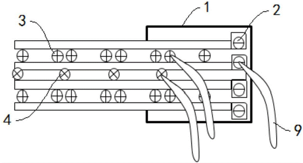
[0032] Such as figure 1 As shown, limited by the area of ​​the test machine 1, the nanoprobe instrument can only test the electrical characteristics of the semiconductor unit within a certain range close to the gate contact 2; for semiconductor units beyond this range, because the drain contact 3 and the source contact 4 cannot be located on the testing machine 1 at the same time as the gate contact 2, so their electrical characteristics cannot be tested with a nanoprobe instrument.

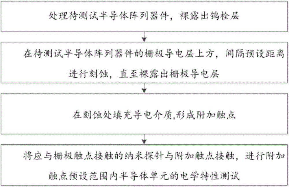
[0033] Such as figure 2 As shown, a semiconductor array device testing method of the present invention comprises the following steps:

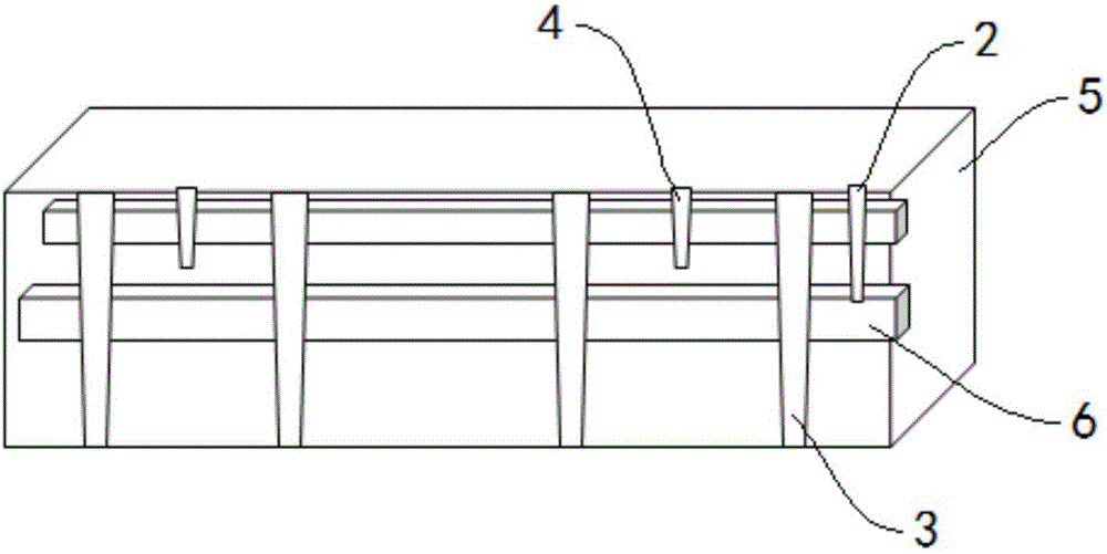
[0034] Step 1, such as image 3 As shown, the semiconductor array device to be tested is proces...


PUM


Abstract

The invention relates to a test method for a semiconductor array device. The test method comprises: a to-be-tested semiconductor array device is processed and a tungsten plug layer is exposed; etching is carried out above a gate conducting layer of the to-be-tested semiconductor array device at a preset interval until the gate conducting layer is exposed; the etched parts are filled with conducting media to form attached contact points; and nano probes that should be in contact with gate contact points are in contact with the attached contact points and electrical characteristic testing of a semiconductor unit within a preset attached contact range is carried out. The method has the following beneficial effects: for semiconductor units, corresponding to drain contact points and source contact points that are not arranged at a testing machine bench with gate contact points simultaneously, attached contact points in conduction with gates are added near the semiconductor units, so that the attached contact points, the drain contact points and the source contact points corresponding to the semiconductor units can be arranged at the testing machine bench simultaneously, so that the electrical characteristic of the semiconductor unit can be tested by using the nano probe testing instrument.

Description

technical field [0001] The invention relates to the technical field of semiconductor testing, in particular to a semiconductor array device testing method. Background technique [0002] In the failure analysis of semiconductor devices, a nanoprobe tester is usually used to test the electrical characteristics of the semiconductor device on the tungsten plug layer of the semiconductor device, and analyze the failure cause of the semiconductor device according to the electrical characteristics. The specific operation is to connect a nanoprobe to the tungsten plug corresponding to the drain, source and gate of the semiconductor device, apply different voltages on the drain, source and gate through the nanoprobe, and obtain the corresponding electrical properties. However, the characteristics of semiconductor array devices (such as memory chips) are: in the tungsten plug layer, each row of semiconductor units shares a gate contact, and the drain contact and source contact are di...

Claims


Application Information

Patent Timeline
IPC IPC(8): G01R31/26G01R1/067
CPCG01R1/06744G01R31/2601
Inventor 张佐兵张顺勇谢振
Owner WUHAN XINXIN SEMICON MFG CO LTD
Why Eureka
Try Eureka