Organic thin-film transistor and manufacturing method thereof

A technology of organic thin film and transistor, which is applied in the field of organic thin film transistor and its manufacturing, can solve the problem of difficult interconnection of the upper and lower electrode layers, and achieve the effect of simple and easy to realize, low cost and low cost

Active Publication Date: 2017-05-24
WUHAN CHINA STAR OPTOELECTRONICS TECH CO LTD
View PDF6 Cites 8 Cited by
  • Summary
  • Abstract
  • Description
  • Claims
  • Application Information

AI Technical Summary

Problems solved by technology

[0006] The technical problem to be solved by the present invention is that the via holes formed from the patterned insulating l

Method used


Image

  • Organic thin-film transistor and manufacturing method thereof
  • Organic thin-film transistor and manufacturing method thereof
  • Organic thin-film transistor and manufacturing method thereof

Examples


Embodiment 1

[0062] In order to solve the technical defect in the existing thin film transistors that it is difficult to interconnect the upper and lower electrode layers through the via holes formed from the patterned insulating layer, the embodiment of the present invention provides an organic thin film transistor with via holes interconnection.

[0063] The via interconnected organic thin film transistor provided in the embodiment of the present invention is a top-gate thin film transistor.

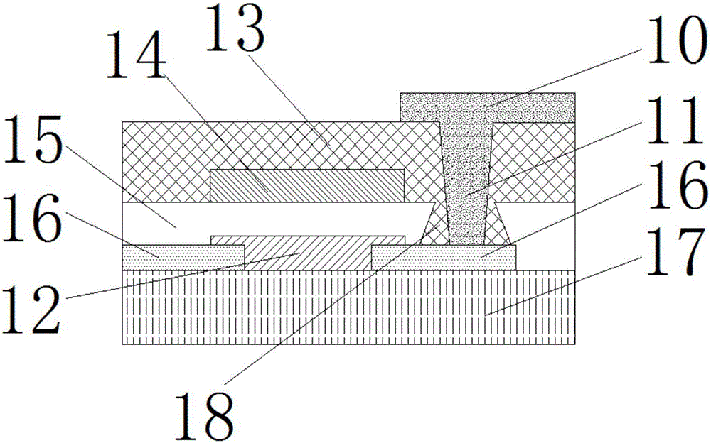
[0064] figure 2 A schematic structural diagram of an organic thin film transistor according to Embodiment 1 of the present invention is shown. Such as figure 2 As shown, the organic thin film transistor of the present embodiment includes:

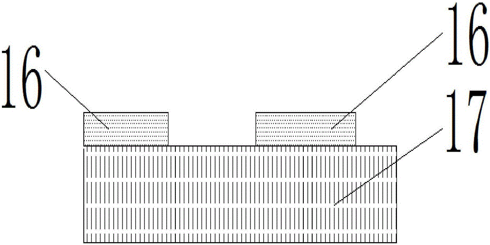
[0065] insulating substrate 17;

[0066] a source-drain electrode layer 16 formed on the insulating substrate 17;

[0067] an organic semiconductor layer 12 formed on the source-drain electrode layer 16;

[0068] A self-patterned organic gate insulating l...

Embodiment 2

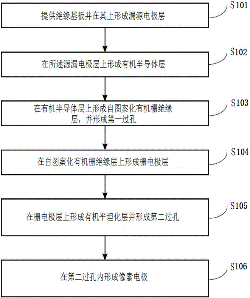
[0083] The embodiment of the present invention also provides a method for manufacturing an organic thin film transistor, which includes:

[0084] Form a multi-layer structure including an insulating substrate 17, a source-drain electrode layer 16, an organic semiconductor layer 12, a self-patterned organic gate insulating layer 15, a gate electrode layer 14, and an organic planarization layer 13; A first via hole 18 is formed in the organic gate insulating layer 15, a second via hole 11 is formed in the organic planarization layer 13, and the second via hole 11 in the organic planarization layer 13 is located in the self-patterned organic and forming the pixel electrode 10 in the second via hole 11 in the organic planarization layer 13 .

[0085] A method for manufacturing an organic thin film transistor, further comprising:

[0086] providing an insulating substrate 17;

[0087] A source-drain electrode layer 16 is formed on the insulating substrate 17; the source-drain ele...

Embodiment 3

[0120] The embodiment of the present invention also provides a method for manufacturing an organic thin film transistor, which includes:

[0121] Form a multi-layer structure including an insulating substrate 17, a source-drain electrode layer 16, an organic semiconductor layer 12, a self-patterned organic gate insulating layer 15, a gate electrode layer 14, and an organic planarization layer 13; A first via hole 18 is formed in the organic gate insulating layer 15, a second via hole 11 is formed in the organic planarization layer 13, and the second via hole 11 in the organic planarization layer 13 is located in the self-patterned organic and forming the pixel electrode 10 in the second via hole 11 in the organic planarization layer 13 .

[0122] A method for manufacturing an organic thin film transistor, further comprising:

[0123] providing an insulating substrate 17;

[0124] A source-drain electrode layer 16 is formed on the insulating substrate 17; the source-drain ele...


PUM

PropertyMeasurementUnit
Thicknessaaaaaaaaaa
Thicknessaaaaaaaaaa
Thicknessaaaaaaaaaa

Abstract

The invention relates to an organic thin-film transistor and a manufacturing method thereof, aiming at solving the problem that the interconnection between an upper electrode layer and a lower electrode layer is harder to realize by a through hole formed in a self-patterned insulating layer in the existing thin-film transistor. The organic thin-film transistor comprises an insulating substrate, a source and drain electrode layer, an organic semiconductor layer, a self-patterned organic gate insulating layer, a gate electrode layer, an organic flattening layer and a pixel electrode. The method comprises the step of forming a multi-layer structure which sequentially comprises the insulating substrate, the source and drain electrode layer, the organic semiconductor layer, the self-patterned organic gate insulating layer, the gate electrode layer and the organic flattening layer. The organic thin-film transistor and the manufacturing method thereof inherit the advantage of the simple process of the self-patterned insulating layer, and solve the problem of disconnection caused in the interconnection process of the upper electrode layer and the lower electrode layer; the organic thin-film transistor can be prepared with low cost.

Description

technical field [0001] The invention relates to the field of manufacturing technology of thin film transistors, in particular to an organic thin film transistor and a manufacturing method thereof. Background technique [0002] With the development of semiconductor technology, video products, especially digital video or image devices have become common products in daily life. In these digital video or image devices, the display is an important component to display relevant information. [0003] In recent years, great progress has been made in the research and application of organic thin film transistor devices, and it has attracted people's attention as a new generation of display technology. Compared with inorganic thin-film transistors, organic thin-film transistors have more advantages: First, there are more newer technologies for making organic thin films, such as Lang-muir-Blodgett (LB) technology, molecular self-assembly technology, vacuum evaporation, spraying, etc. ...

Claims


Application Information

Patent Timeline
IPC IPC(8): H01L51/05H01L51/40H01L21/768
CPCH01L21/76804H01L21/76895H01L2221/101H10K10/468H10K10/464
Inventor 谢应涛
Owner WUHAN CHINA STAR OPTOELECTRONICS TECH CO LTD
Why Eureka
Try Eureka