Via hole bent miniaturized PCB_RFID antenna

A technology of vias and antennas, applied in the field of RFID antennas, can solve the problems of single form, too large size of RFID antennas, and lack of aesthetic feeling, and achieve the effect of good performance and reduced size

Pending Publication Date: 2017-05-24
CHINA JILIANG UNIV
View PDF6 Cites 0 Cited by
  • Summary
  • Abstract
  • Description
  • Claims
  • Application Information

AI Technical Summary

Problems solved by technology

Although it has been processed by single-sided bending technology, the size of the RFID antenna is still slightly too large for electronic products with a high degree of integration, and the single form is not aesthetically pleasing

Method used


Image

  • Via hole bent miniaturized PCB_RFID antenna
  • Via hole bent miniaturized PCB_RFID antenna
  • Via hole bent miniaturized PCB_RFID antenna

Examples


Embodiment Construction

[0018] The present invention will be further described below in conjunction with accompanying drawing.

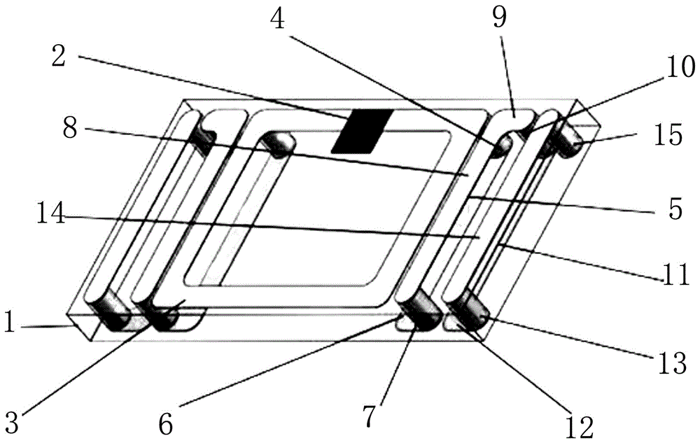
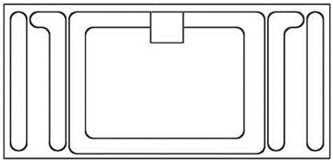
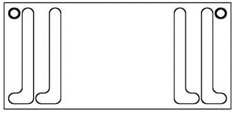
[0019] like Figure 1-3 As shown, the miniaturized PCB RFID antenna bent via holes of the present invention includes a PCB substrate 1, which is made of polyimide or glass fiber epoxy resin material, with a length of 20 mm, a width of 10 mm, and a thickness of 1.6 mm. mm. The antenna is fed by the feeder chip 2 above the substrate, and is symmetrical about the vertical midline of the feeder chip 2, so only the right half of the PCB RFID antenna is marked, and the structural parameters of the left half are exactly the same, and the length of the feeder chip is and width are both 2mm. The matching ring 3 is located on the upper surface of the PCB substrate 1, above it is connected to both sides of the feed chip, the height is 0.035mm-0.036mm, the length of the outer ring is 11mm-12mm, the width of the outer ring is 9mm-9.5mm, and the length of the inner ring is 9mm-10mm, t...


PUM


Abstract

The invention discloses a via hole bent miniaturized PCB_RFID antenna, which comprises a PCB substrate, a feed chip and a mating ring. The mating ring is located on the upper surface of the PCB substrate. The top of the mating ring is connected with the two sides of the feed chip. The upper right corner of the mating ring is connected with a first upper through hole. The bottom end of the first upper through hole is connected with a first lower vertical wiring. The right lower part of the first lower vertical wiring is connected with a first lower transverse wiring. The right side of the first lower transverse wiring is connected with a first lower through hole. The top end of the first lower through hole is connected with a first upper vertical wiring. The right upper part of the first upper vertical wiring is connected with a first upper transverse wiring. The right side of the first upper transverse wiring is connected with a second upper through hole. The bottom end of the second upper through hole is connected with a second lower vertical wiring. The right lower part of the second lower vertical wiring is connected with a second lower transverse wiring. The right side of the second lower transverse wiring is connected with a second lower through hole. The top end of the second lower through hole is connected with a second upper vertical wiring. The top end of the second upper vertical wiring is connected with a third upper through hole.

Description

technical field [0001] The invention belongs to the field of RFID antennas, in particular to a through-hole bending miniaturized PCB RFID antenna. Background technique [0002] With the development of the Internet of Things, RFID technology has been applied in various fields. RFID technology is a key technology in the Internet of Things. It is a wireless communication technology that can realize non-contact automatic identification between RFID electronic tags and readers through electromagnetic field propagation. The antenna is the most important part of the RFID system. The antenna and the chip together form the RFID electronic tag, which is widely used in various fields to identify items. The manufacturing industry adopts RFID technology extensively when implementing the smart manufacturing strategy. As an indispensable part of the manufacturing industry, electronic products are characterized by small size and complex types. To identify. In order to facilitate the info...

Claims


Application Information

Patent Timeline
Patent Type & Authority Applications(China)
IPC IPC(8): H01Q1/38H01Q1/50H01Q9/27H01Q1/22
CPCH01Q1/2208H01Q1/38H01Q1/50H01Q9/27
Inventor 洪涛张松蒋天齐
Owner CHINA JILIANG UNIV
Why Eureka
Try Eureka