Organic light-emitting diode device and production method thereof

A light-emitting diode, organic technology, applied in the direction of organic semiconductor devices, chemical instruments and methods, semiconductor/solid-state device manufacturing, etc., can solve the problems of reducing water vapor barrier ability, film shedding, non-bending, etc., to ensure gas barrier effect, Excellent water and oxygen barrier ability and low water vapor transmission rate

Inactive Publication Date: 2017-06-09
AAC TECH NANJING
View PDF5 Cites 21 Cited by
  • Summary
  • Abstract
  • Description
  • Claims
  • Application Information

AI Technical Summary

Problems solved by technology

The organic light-emitting diode device formed has excellent water-oxygen gas barrier ability, WVTR<10E-6g/m2/day, but has the following defects: the thickness is relatively thick, up to 0.5-0.7mm, the process is relatively complicated, and the preparation process requires High temperature conditions may have an impact on the cathode of the OLED unit, and the resulting organic light-emitting diode device has the characteristics of poor flexibility and cannot be bent
However, thin-film packaging technology cannot completely solve the problem of water and oxygen penetration. First, because the inorganic thin film is formed by CVD film-forming process, specifically, it is a chemical gas phase reaction triggered by plasma plasma, and active molecules diffuse and adsorb on the substrate to form islands. Forming a continuous film, the process will inevitably produce pinholes and gaps, thereby

Method used


Image

  • Organic light-emitting diode device and production method thereof
  • Organic light-emitting diode device and production method thereof
  • Organic light-emitting diode device and production method thereof

Examples


Embodiment Construction

[0035] The present invention will be further described below in conjunction with the accompanying drawings and embodiments.

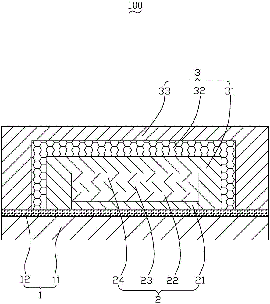
[0036] see figure 1 , is a schematic structural view of the organic light emitting diode device provided by the present invention. The OLED device 100 includes a substrate 1 , an OLED unit 2 disposed on the substrate 1 and an encapsulation structure 3 , the encapsulation structure 3 is connected to the substrate 1 for encapsulating the OLED unit 2 .

[0037] The substrate 1 includes a substrate 11 and a conductive anode 12 deposited on the substrate 11 . The substrate 11 is a rigid substrate or a flexible substrate, wherein the rigid substrate is glass, silicon wafer or other rigid materials; the flexible substrate is a plastic substrate, aluminum foil, ultra-thin metal or ultra-thin glass. The conductive anode 12 is formed of ITO, graphene, indium gallium zinc oxide or other conductive materials, and is deposited on the surface of the substrate 11 by...


PUM

PropertyMeasurementUnit
Thicknessaaaaaaaaaa

Abstract

The invention discloses an organic light-emitting diode device. The light-emitting diode device comprises a substrate; an OLED unit disposed on the substrate; and a packaging structure, which is connected with the substrate, and is used for packaging the OLED unit. The packaging structure comprises a first inorganic barrier layer disposed on the outer side of the OLED unit in a wrapped manner, an inorganic nanometer-organic copolymer mixing layer disposed on the outer side of the first inorganic barrier layer in a wrapped manner, and a second inorganic barrier layer disposed on the outer side of the inorganic nanometer-organic copolymer mixing layer in a wrapped manner. The organic light-emitting diode device has advantages of good water oxygen barrier performance, thin thickness, and strong interface bonding force. The invention also provides the production method of the organic light-emitting diode device.

Description

[0001] 【Technical field】 [0002] The invention relates to the technical field of light emitting diodes, in particular to an organic light emitting diode device and a manufacturing method thereof. [0003] 【Background technique】 [0004] Organic Light-Emitting Diode (OLED) devices can be used as light sources for display devices and lighting devices. The organic light emitting diode device mainly includes a substrate, an OLED unit disposed on the substrate, and an encapsulation structure for encapsulating the OLED unit. The function of the encapsulation structure is to block the penetration of water and oxygen molecules, so as to prevent the damage of the OLED unit. [0005] OLED unit encapsulation usually adopts two methods, one is encapsulation lid encapsulation technology, and the other is thin film encapsulation technology. Among them, the encapsulation technology of the encapsulation cover is to carry out the dispensing process on the encapsulation cover, and then carry ...

Claims


Application Information

Patent Timeline
IPC IPC(8): H01L51/52H01L51/56
CPCH10K50/844H10K2102/331H10K71/00B32B27/08H10K50/846
Inventor 谢再锋黄达曹辰辉
Owner AAC TECH NANJING
Why Eureka
Try Eureka