Semiconductor device and method for manufacturing same

A manufacturing method and semiconductor technology, applied in the direction of semiconductor/solid-state device manufacturing, electrical components, circuits, etc., can solve the problems of accuracy impact, impact on device performance, unclear overlay pattern, etc., to reduce thickness and light transmittance. Enhanced, more accurate effects

Inactive Publication Date: 2016-06-01
INST OF MICROELECTRONICS CHINESE ACAD OF SCI
View PDF6 Cites 1 Cited by
  • Summary
  • Abstract
  • Description
  • Claims
  • Application Information

AI Technical Summary

Problems solved by technology

[0004] In the manufacturing process of the device, when the first metal layer is made, the metal layer becomes thicker. Due to the poor light transmission of the metal layer, the overlay pattern of t

Method used


Image

  • Semiconductor device and method for manufacturing same
  • Semiconductor device and method for manufacturing same
  • Semiconductor device and method for manufacturing same

Examples


Example Embodiment

[0024] The embodiments of the present invention are described in detail below. Examples of the embodiments are shown in the accompanying drawings, in which the same or similar reference numerals indicate the same or similar elements or elements with the same or similar functions. The embodiments described below with reference to the accompanying drawings are exemplary, and are only used to explain the present invention, and cannot be construed as limiting the present invention.

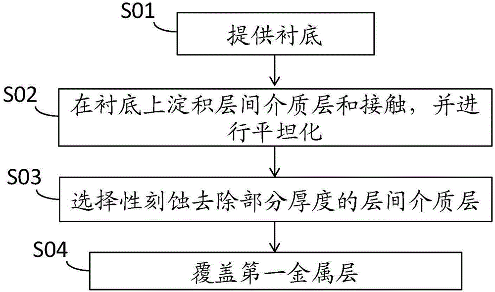
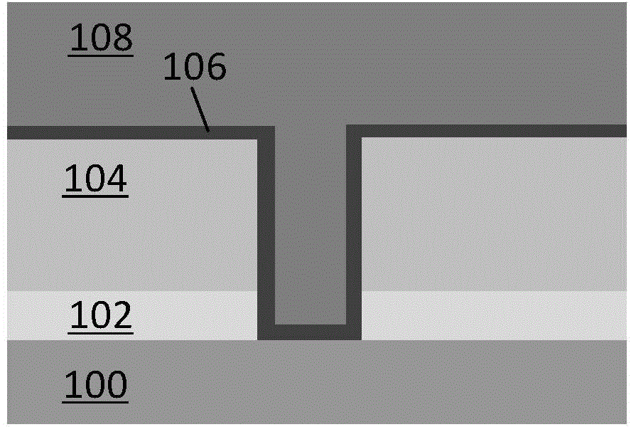
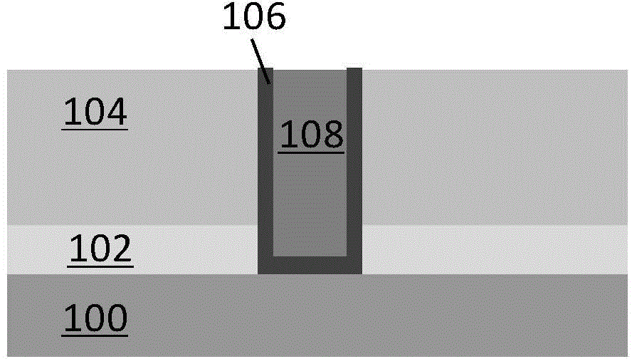
[0025] In the present invention, a method for manufacturing a semiconductor device is provided, which includes the steps of: providing a substrate; depositing an interlayer dielectric layer and a contact layer on the substrate and performing planarization; and selectively etching and removing a part of the thickness of the layer Intermediate layer; covering the first metal layer.

[0026] In the present invention, after the interlayer dielectric layer and the contact layer are deposited and planarized, a p...


PUM

PropertyMeasurementUnit
Thickness rangeaaaaaaaaaa

Abstract

The invention provides a method for manufacturing a semiconductor device. The method comprises steps of: providing a substrate; depositing and planarizing an interlayer dielectric layer and a contact layer on the substrate; selectively etching and removing the interlayer dielectric layer with a certain thickness; and covering a first metallic layer. A step height difference is formed between the contact layer and the interlayer dielectric layer so that the thickness of the first metallic layer on the contact layer is reduced. Therefore, local transmittance is enhanced and aligning accuracy is increased when the first metallic layer is subjected to photoetching.

Description

technical field [0001] The invention relates to the field of semiconductor manufacturing, in particular to a semiconductor device and a manufacturing method thereof. Background technique [0002] In the current semiconductor manufacturing process, dozens of lithography processes are required. In the lithography process, the resolution of the lithography machine and the accuracy of alignment will affect the accuracy of the lithography process. [0003] Usually, an overlay pattern is formed on the non-device formation area, which is used as an alignment mark when the pattern of the lower layer is fabricated. [0004] In the manufacturing process of the device, when the first metal layer is made, the metal layer becomes thicker. Due to the poor light transmission of the metal layer, the overlay pattern of the front layer is not clear. When the photolithography of the metal layer is performed, The accuracy of the alignment to the front layer is affected, affecting the performan...

Claims


Application Information

Patent Timeline
IPC IPC(8): H01L21/3105
Inventor 唐波闫江王红丽许静唐兆云徐烨锋李春龙杨萌萌
Owner INST OF MICROELECTRONICS CHINESE ACAD OF SCI
Why Eureka
Try Eureka