GaN-based VCSEL chip based on porous DBR and preparation method

A chip and current confinement layer technology, applied in laser parts, electrical components, lasers, etc., can solve the problems of complex device process, high cost, and lower quality factor of resonator, and achieve simple and repeatable process Effect

A chip and current confinement layer technology, applied in laser parts, electrical components, lasers, etc., can solve the problems of complex device process, high cost, and lower quality factor of resonator, and achieve simple and repeatable process Effect

CN106848838AActive Publication Date: 2017-06-13INST OF SEMICONDUCTORS - CHINESE ACAD OF SCI

Image

  • GaN-based VCSEL chip based on porous DBR and preparation method
  • GaN-based VCSEL chip based on porous DBR and preparation method
  • GaN-based VCSEL chip based on porous DBR and preparation method

Examples


Embodiment Construction

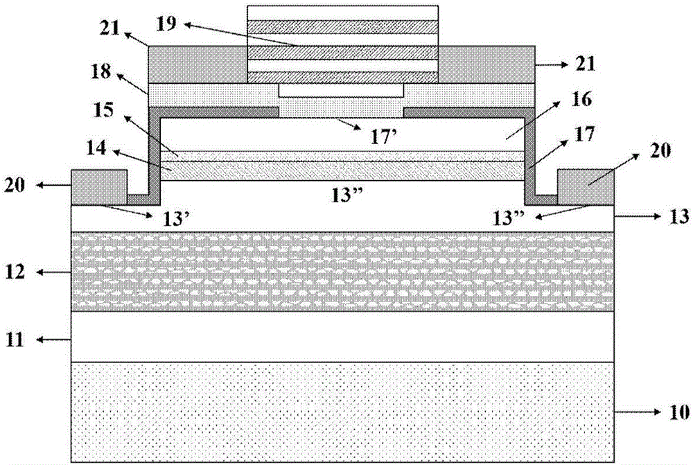
[0035] see figure 1 , the present invention provides a GaN-based VCSEL chip based on porous DBR, comprising:

[0036] A substrate 10 is a plane or pattern substrate, and the material of the substrate 10 is sapphire, silicon or silicon carbide;

[0037] A buffer layer 11, which is made on the upper surface of the substrate 10, the buffer layer is composed of a low-temperature GaN nucleation layer and an unintentionally doped GaN layer, using high-purity ammonia as a nitrogen source, trimethylgallium or triethylgallium As the Ga source, the GaN nucleation layer is grown at low temperature first, and then the unintentionally doped GaN layer is grown at high temperature. Materials that can be used as the nucleation layer also include AlN, ZnO or graphene;

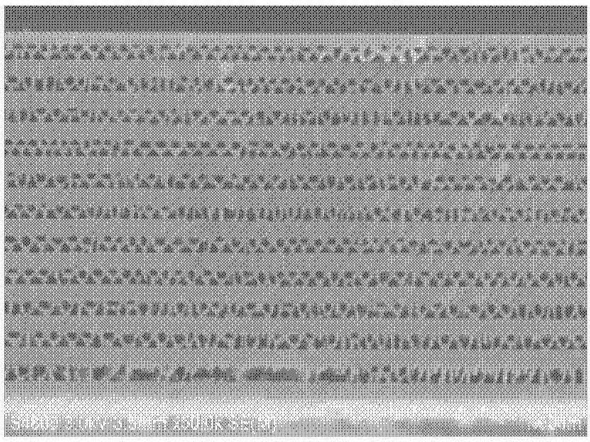
[0038] A bottom porous DBR layer 12, which is made on the upper surface of the buffer layer 11, the material of the bottom porous DBR layer 12 is GaN, AlGaN, InGaN or AlInGaN, or a combination of the above materials. Porous l...


PUM

PropertyMeasurementUnit
reflectanceaaaaaaaaaa

Abstract

The invention discloses a GaN-based VCSEL chip based on a porous DBR. The GaN-based VCSEL chip comprises a substrate, a buffer layer manufactured on the substrate, a bottom porous DBR layer manufactured on the buffer layer, an n-type doped GaN layer manufactured on the bottom porous DBR layer, an active layer manufactured on the n-type doped GaN layer, an electron blocking layer manufactured on the active layer, a p-type doped GaN layer manufactured on the electron blocking layer, a current limiting layer manufactured on the p-type doped GaN layer, a transparent electrode manufactured on the p-type doped GaN layer, an n electrode, a p electrode manufactured on the transparent electrode, and a dielectric DBR layer, wherein a table board is formed by etching the periphery of the n-type doped GaN layer downwards; a current window is formed in the center of the current limiting layer; the current limiting layer covers the active layer, the electron blocking layer and the side wall of a bulge part of the n-type doped GaN layer; the n electrode is manufactured on the table board of the n-type doped GaN layer; a notch is formed in the middle of the p electrode; and the dielectric DBR layer is manufactured on the transparent electrode in the notch of the p electrode.

Description

technical field [0001] The invention belongs to the field of laser light sources, in particular to a GaN-based VCSEL (vertical cavity surface emitting laser), in particular to a GaN-based VCSEL chip based on a porous DBR bottom reflector and a preparation method. Background technique [0002] GaN semiconductor-based lasers have shown great application prospects and market demand in high-density optical storage, laser lighting, laser display, visible light communication and other fields, and have attracted much attention in international scientific research and industry in recent years. At present, GaN basal edge-emitting lasers have been commercialized, but vertical cavity surface-emitting lasers (VCSELs) with better performance have not yet reached the practical level. Compared with traditional edge-emitting lasers, GaN-based VCSELs have good dynamic single-mode and spatial emission mode characteristics, low operating threshold, small beam divergence angle, low manufacturin...

Claims


Application Information

Patent Timeline
13 Jun 2017
Publication
CN106848838A
IPC
H01S5/183; H01S5/187
CPC
H01S5/18305; H01S5/18313; H01S5/187; H01S5/34333; H01S5/04257; H01S5/18341; H01S5/18361; H01S5/04253
Inventors
杨超; 刘磊