A grating coupler
A grating coupler, grating technology, applied in the coupling of optical waveguides, instruments, light guides, etc., can solve the problem of low coupling efficiency of grating couplers, and achieve the effect of improving coupling efficiency and simple and convenient preparation process.
- Summary
- Abstract
- Description
- Claims
- Application Information
AI Technical Summary
Problems solved by technology
Method used
Image

Examples
Embodiment 1
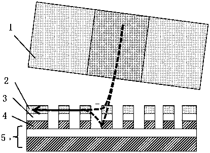
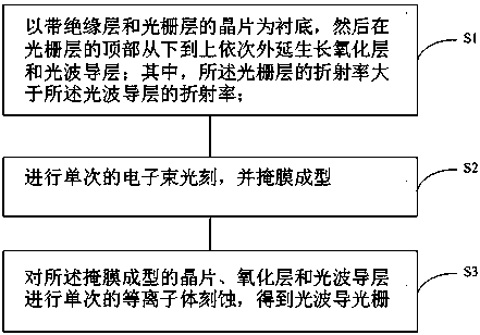
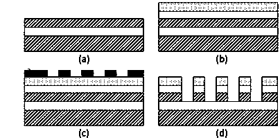
[0034] figure 1 It is a schematic structural diagram of a grating coupler according to an embodiment. Such as figure 1 Described, a kind of grating coupler, comprises: from bottom to top successively with the wafer with insulating layer 5 and grating layer 4, oxide layer 3 and optical waveguide layer 2; Refractive index; the grating layer 4 and the optical waveguide layer 2 are grating structures with a preset period; the grating layer 4 on the insulating layer 5 is used as a distributed Bragg grating reflector, and the optical waveguide layer 2 converts the The optical signal is vertically coupled into the grating coupler; during the process of optical coupling into the grating coupler, part of the light is directly coupled into the optical waveguide layer 2, and the other part of the light passes through the oxide layer 3 and irradiates the distributed Bragg grating reflector, and is absorbed by the Bragg grating The reflection mirror reflects back to the optical waveguide...
Embodiment 2
[0038] On the basis of Embodiment 1, this embodiment further defines its various components, specifically:
[0039] The grating layer on the insulating layer is a silicon grating layer, and the optical waveguide layer is a silicon nitride optical waveguide layer; the silicon wafer on the insulating layer is used as a distributed Bragg grating reflector, and the silicon nitride optical waveguide layer The optical signal in the optical fiber is vertically coupled into the grating coupler; during the process of optical coupling into the grating coupler, part of the light is directly coupled into the silicon nitride optical waveguide layer, and the other part of the light passes through the oxide layer and irradiates the distributed Bragg grating reflector , and is reflected back to the silicon nitride optical waveguide layer by the Bragg grating mirror. In this embodiment, since the single crystal silicon material has a relatively high refractive index (n=3.42) in the communicati...
Embodiment 3
[0041] On the basis of Embodiment 1, this embodiment further defines its various components, specifically:
[0042] The grating layer on the insulating layer is a gallium arsenide wafer or an indium phosphide wafer, and the optical waveguide layer is a preset ratio of silicon oxynitride and silicon oxide optical waveguide layers; the gallium arsenide or silicon oxide optical waveguide layer on the insulating layer is The indium phosphide wafer is used as a distributed Bragg grating reflector, and the silicon oxynitride and silicon oxide optical waveguide layers with the preset ratio vertically couple the optical signal in the optical fiber into the grating coupler; during the process of light coupling into the grating coupler , a part of the light is directly coupled into the silicon oxynitride and silicon oxide optical waveguide layer with a preset ratio, and the other part of the light is irradiated through the oxide layer to the distributed Bragg grating reflector, and is re...
PUM
 Abstract
Description
Claims
Application Information
PatSnap Eureka turns technology decisions into work you can execute. Powered by our Innovation Knowledge Graph, it runs expert workflows across engineering, life sciences, materials and intellectual property. Get your review-ready output in minutes.


