Laser structure for grating coupling and packaging method

A laser and optical waveguide technology, applied in the field of communication, can solve the problems of complex structure, difficulty in improving the production efficiency of assembly process, and many parts, and achieve the effect of high coupling efficiency, low cost, and simple structural design

Active Publication Date: 2016-12-07
GUANGXUN SCI & TECH WUHAN
View PDF5 Cites 25 Cited by
  • Summary
  • Abstract
  • Description
  • Claims
  • Application Information

AI Technical Summary

Problems solved by technology

For the light source input of this kind of grating coupler, Luxtera has been involved in the US patent application publication US201414324544A1. The entire laser light source part is composed of multiple discrete parts such as laser chips, lenses, isolators, and reflectors. The zeros involved Many components and complex structures make it difficult to improve the production efficiency of the assembly process

Method used


Image

  • Laser structure for grating coupling and packaging method
  • Laser structure for grating coupling and packaging method
  • Laser structure for grating coupling and packaging method

Examples


Embodiment Construction

[0037] In order to make it easier for those skilled in the art to understand and implement the present invention, the present invention will be further described in detail below in conjunction with the accompanying drawings and specific embodiments.

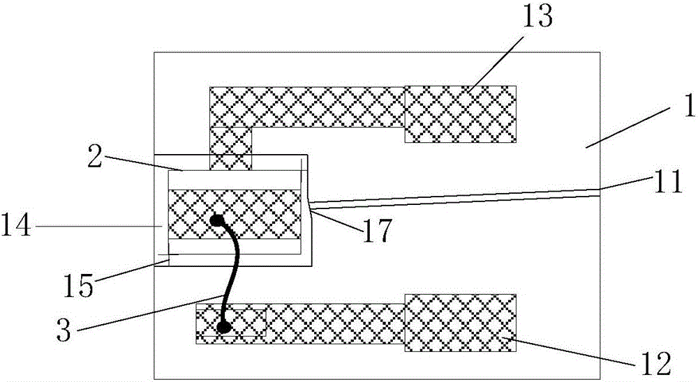
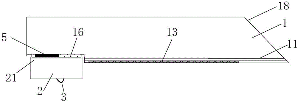
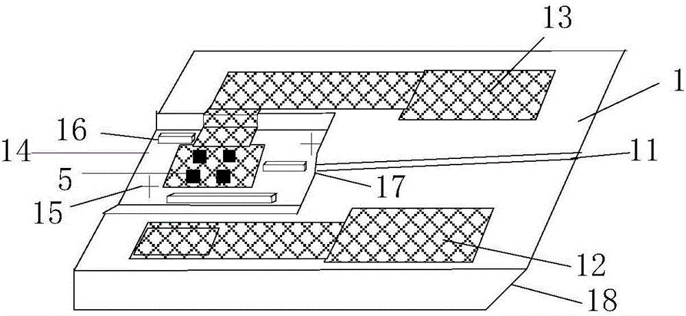
[0038] The structure of the laser provided by the present invention is as Figure 1-3 As shown, it includes two parts: substrate 1 and laser chip 2; wherein, substrate 1 includes optical waveguide 11, electrode 12 and electrode 13, etched groove 14, alignment mark 15, height positioning block 16 ( figure 1 Not shown in ), coupling surface 17, reflective surface 18, one end of substrate 1 is provided with at least partially etched groove 14 for accommodating laser chip 2, the other end of substrate 1 is provided with reflective surface 18 (i.e. light exit surface), the optical waveguide 11 extends between the etched groove 14 and the reflective surface 18, the reflective surface 18 is used to change the light output direction of t...


PUM


Abstract

The invention relates to a laser component, which comprises a substrate and a laser chip, wherein the laser chip is provided with an active region for generating and outputting laser light, and an electrode for supplying the laser chip with electricity; an etching groove for at least partially accommodating the laser chip is formed in one end of the substrate and a light-exiting surface is arranged at the other end of the substrate; the substrate is also provided with an optical waveguide which extends between the etching groove and the light-exiting surface; the laser chip is arranged in the etching groove of the substrate; and the active region of the laser chip is aligned at the optical waveguide on the substrate. The laser component only comprises two parts, namely the substrate for integrating the optical waveguide and the electrode and the laser chip, and is free of other discrete component. The laser structure is simple in design and low in cost; a flip chip bonding alignment technology can be adopted to achieve coupling of a laser light path and coupling of a laser and a grating coupler of a silicon photonic integrated chip; and a passive alignment technology is adopted, so that the coupling efficiency is high and the laser component is suitable for high-efficiency mass production.

Description

technical field [0001] The invention relates to a laser component for optical fiber communication, in particular to a laser structure and packaging method for grating coupling, and in particular to a method for realizing the coupling of a laser light source and a grating coupler in a silicon photonic device. The invention belongs to the field of communication. Background technique [0002] Silicon photonic materials, due to their high integration, good high-frequency characteristics, low power consumption, and compatibility with existing large-scale integrated circuit processes, have become a research hotspot in the world. Various silicon photonic devices such as high-speed electro-optical modulators, photoelectric detectors Devices and integrated chips have emerged and gradually matured. [0003] Since silicon material is an indirect semiconductor material, it is difficult to make the material itself into a laser element. Therefore, an external III-IV laser is generally use...

Claims


Application Information

Patent Timeline
Patent Type & Authority Applications(China)
IPC IPC(8): H01S5/022G02B6/42
CPCG02B6/4296H01S5/0225H01S5/0237H01S5/02375G02B6/34G02B6/42H01S5/026
Inventor 宋琼辉杜巍马洪勇
Owner GUANGXUN SCI & TECH WUHAN
Why Eureka
Try Eureka