Silicon waveguide spot size converter based on multilayer polymer structure and preparation method thereof

A mode spot converter and silicon waveguide technology, which is applied to optical waveguides, light guides, instruments, etc., can solve the problem of low coupling efficiency between mode spot converters and ordinary single-mode fibers, and facilitate large-scale optical circuit integration and improve coupling. Efficiency and the effect of improving the matching degree of mode spot

Pending Publication Date: 2018-06-08
苏州易缆微光电技术有限公司
View PDF0 Cites 26 Cited by
  • Summary
  • Abstract
  • Description
  • Claims
  • Application Information

AI Technical Summary

Problems solved by technology

[0006] The present invention proposes a silicon waveguide mode spot converter based on a multilayer polymer structure and its preparation method to solve the problem of low coupling efficiency between the mode spot converter and ordinary single-mode optical fiber in the prior art, and realize the improvement of silicon waveguide mode Coupling Efficiency of Spot Converter

Method used


Image

  • Silicon waveguide spot size converter based on multilayer polymer structure and preparation method thereof
  • Silicon waveguide spot size converter based on multilayer polymer structure and preparation method thereof
  • Silicon waveguide spot size converter based on multilayer polymer structure and preparation method thereof

Examples


Embodiment 1

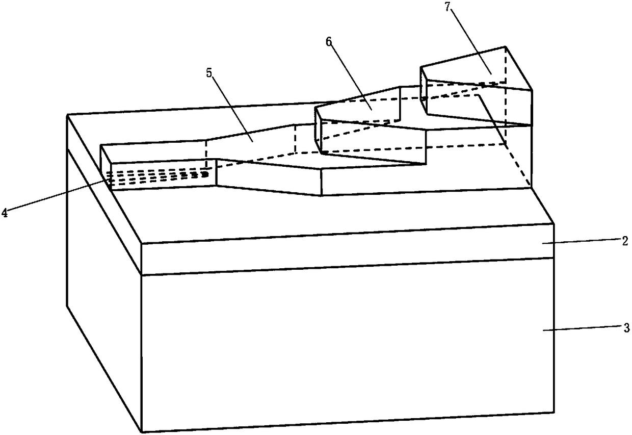
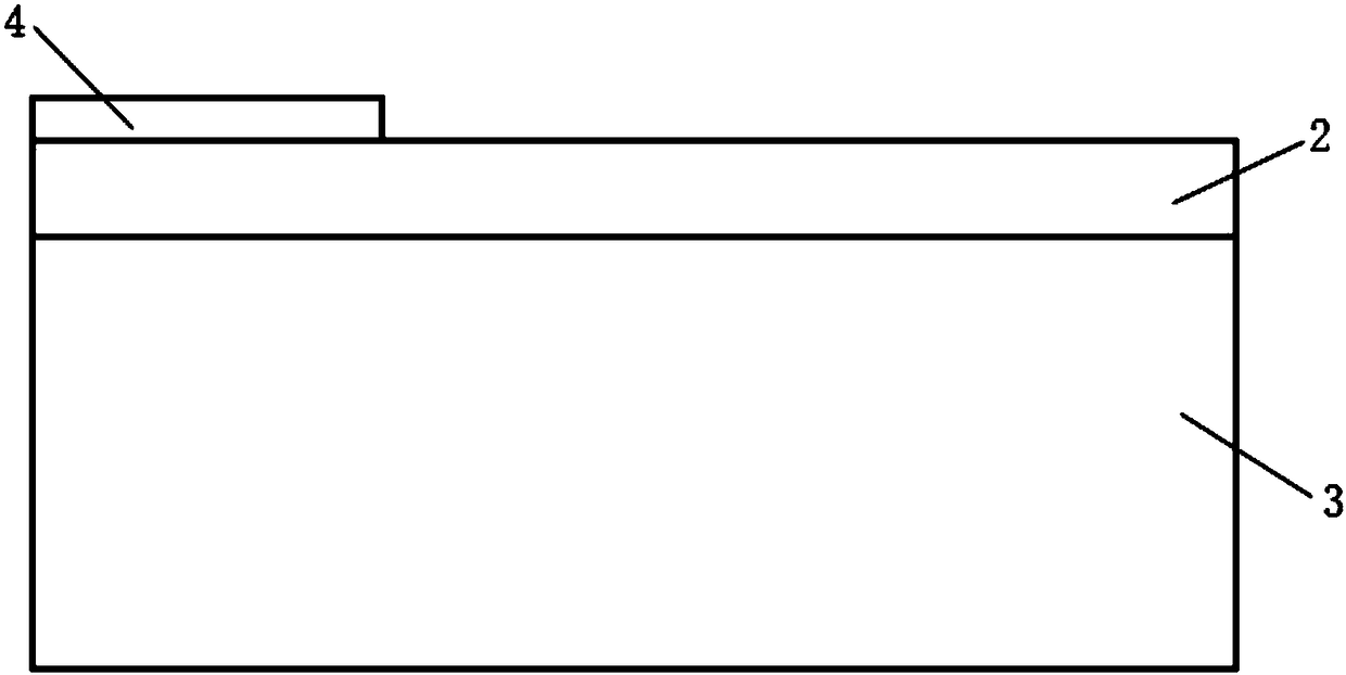
[0049] Such as figure 1 , Figure 15As shown, in this embodiment, a silicon waveguide mode spot converter based on a multilayer polymer structure includes an upper cladding layer 1, an insulator layer 2, a substrate 3, a first optical waveguide 4, a second optical waveguide 5, and a third optical waveguide. Optical waveguide 6 , fourth optical waveguide 7 , support body 8 . In a common silicon photonics chip, the thickness of the insulator layer 2 is usually between 1-5um, and the thickness of the first optical waveguide 4 is usually below 500nm.

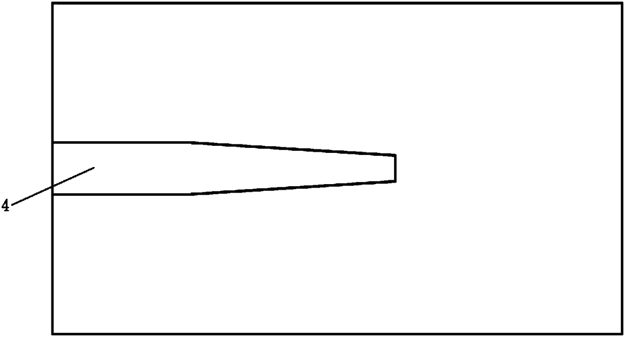
[0050] In the silicon waveguide mode speckle converter based on the multilayer polymer structure described in this embodiment, the substrate 3 is silicon, and the insulator layer 2 is fabricated on the substrate 3. A first optical waveguide 4 is fabricated on the surface of the insulator layer 2 , and the material of the first optical waveguide 4 is silicon, which includes a section of reverse tapered optical waveguide and is plac...

Embodiment 2

[0052] This embodiment provides a method for preparing the above-mentioned silicon waveguide mode spot converter based on a multilayer polymer structure, and the specific steps are as follows:

[0053] (1) growing an insulator layer on the substrate;

[0054] (2) On the silicon substrate on the insulator layer, the first optical waveguide is manufactured by using an integrated microelectronic process such as electron beam lithography or deep ultraviolet exposure and dry etching. After this step is completed, its structure is as follows figure 2 , 3 , 4 shown.

[0055] (3) The second optical waveguide is made on the chip obtained in step 2 by means of spin coating, photolithography, and development, and supports 8a distributed on the left and right sides of the second optical waveguide are produced. After this step is completed, its structure Such as Figure 5 , 6 , 7 shown.

[0056] (4) Fabricate a third optical waveguide on the chip obtained in step 3 by means of spin ...


PUM

PropertyMeasurementUnit
thicknessaaaaaaaaaa

Abstract

The present invention discloses a silicon waveguide spot size converter based on a multilayer polymer structure and a preparation method thereof. The silicon waveguide spot size converter based on themultilayer polymer structure and the preparation method thereof are applied to coupling of silicon nanowire optical waveguides and common single-mode fibers. The structure is made by employing an integrated photoelectron process method, on a silicon substrate on an insulator layer, a taper-type silicon waveguide is made, a lithography technology is employed to continuously nest three layers of combined taper-type optical waveguides with materials of SU-8 photoresist on the insulator layer, and a silicon dioxide upper cladding is deposited to achieve making of a spot size converter. The taper-type portions of the three layers of combined taper-type optical waveguides with materials of SU-8 photoresist are employed to reduce the sizes of spot sizes entering the single-mode fibers in a horizontal direction and a vertical direction, perform cascade with a reverse taper-type silicon waveguide and finally allow a light field to couple into the silicon nanowire optical waveguides. The directend face connection between the silicon nanowire optical waveguides and the common single-mode fibers can be achieved, the matching with the single-mode fiber spot size is improved, the optical coupling efficiency is improved, and it is convenient to perform large-scale optical path integration.

Description

technical field [0001] The invention belongs to the technical field of optical communication and optical interconnection, and more specifically relates to a silicon waveguide mode-spot converter based on a multilayer polymer structure and a preparation method thereof, which are used to solve the interface between a silicon-based photonic chip and a common single-mode optical fiber question. Background technique [0002] Due to the use of a relatively mature CMOS process, the optical integration technology based on silicon-based platforms can provide a low-loss, high-performance solution for optical interconnection. The SOI platform with high refractive index difference is conducive to the establishment of integrated optical devices with smaller size and higher integration level, so it has always received extensive attention. However, for silicon-based photonic chips, an urgent problem to be solved is how to achieve low-loss coupling between small-sized on-chip optical signa...

Claims


Application Information

Patent Timeline
Patent Type & Authority Applications(China)
IPC IPC(8): G02B6/14G02B6/122G02B6/13
CPCG02B6/14G02B6/122G02B6/13
Inventor 秦子翔彭超张仙刘洋温雪沁刘柳陈伟
Owner 苏州易缆微光电技术有限公司
Why Eureka
Try Eureka