Structured light illuminating microscopic imaging system based on integrated photonic chip

A technology of structured light illumination and integrated photons, which is applied in the field of super-resolution microscopic imaging system, can solve the problems of imaging stability, high imaging precision, time accuracy, low signal-to-noise ratio, inconvenient portability, etc., and achieve structural Compact, fast response time, small size effect

Active Publication Date: 2015-03-25
INST OF SEMICONDUCTORS - CHINESE ACAD OF SCI
View PDF8 Cites 26 Cited by
  • Summary
  • Abstract
  • Description
  • Claims
  • Application Information

AI Technical Summary

Problems solved by technology

[0010] However, this solution still uses spatial light modulation to obtain structured light, which has a complex structure and a large volume.
not portable
[0011] In summary, the microscopic imaging system in the prior art still fails to solve the problems of imaging stability, high imaging precision and phase accuracy, time accuracy and low signal-to-noise ratio in the synchronization process.

Method used


Image

  • Structured light illuminating microscopic imaging system based on integrated photonic chip
  • Structured light illuminating microscopic imaging system based on integrated photonic chip
  • Structured light illuminating microscopic imaging system based on integrated photonic chip

Examples


Embodiment 1

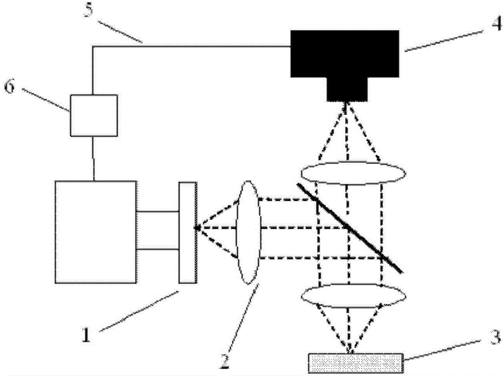
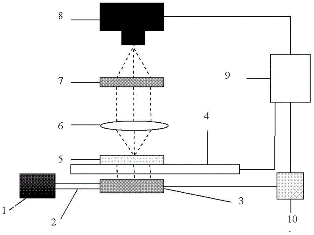
[0036] Embodiment 1: as figure 2 , 3 As shown, a structured illumination microscopic imaging system based on an integrated photonic chip, including a light source 1, an integrated photonic chip 3, a sample placement table 4, a microscope objective lens 6, an optical filter 7, a photoelectric detector 8, and a computer processing system 9 and the control system 10, the light source 1 is connected to the integrated photonic chip 3, the integrated photonic chip 3 is arranged under the sample placement platform 4, the microscopic objective lens 6 is arranged above the sample placement platform 5, and the optical filter 7 is arranged above the microscopic objective lens 6, The photodetector 8 is located above the filter 7; the sample placement platform 4 is fixed with the sample 5 to be tested, and the sample placement platform 4 holds a glass slide, and the slide glass is the sample 5 to be tested, and the sample placement platform 4 is Transparent; the light emitted by the ligh...

Embodiment 2

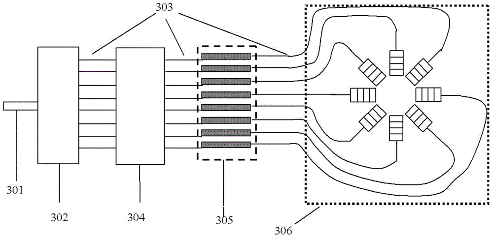
[0043] Embodiment 2: as image 3 As shown, the integrated photonic chip structure adopted in the present invention includes a grating coupler 301, an optical beam splitter 302, an optical waveguide 303, an optical switch array 304, an optical phase shifting array 305 and a grating diffraction array 306 integrated into a millimeter-scale chip . The input light enters the 1×3 beam splitter 302 through the grating coupler 301 and becomes three beams with equal power, and then enters the 3×8 optical switch array and is output from the specified output port. The phase shifting array 305 is used to control the phases of the three light beams entering the diffraction grating array 306 respectively. After being diffracted by the grating, the three beams interfere in the space perpendicular to the surface of the chip to form a three-dimensional structured light with a specific periodic distribution.

Embodiment 3

[0044] Embodiment 3: as Figure 4 Shown is a schematic diagram of the arrangement of the light diffraction array used in the present invention. Figure 4 a is arranged in a linear array, Figure 4 b is a polyline array arrangement, Figure 4 c is arranged in a curved array.


PUM


Abstract

The invention discloses a structured light illuminating microscopic imaging system based on an integrated photonic chip. The structured light illuminating microscopic imaging system comprises a light source, the integrated photonic chip, a sample containing table, a microobjective, a filter part, a photoelectric detector, a computer processing system and a control system. The light source is connected with the integrated photonic chip, the integrated photonic chip is arranged below the sample containing table, the microobjective is arranged above the sample containing table, the filter part is arranged above the microobjective, and the photoelectric detector is arranged above the filter part. A sample to be detected is fixed to the sample containing table, and light emitted by the light source irradiates the sample to be detected on the sample containing table after being processed by the integrated photonic chip. The computer processing system is connected with the sample containing table, the photoelectric detector and the control system. The integrated photonic chip is connected with the control system. According to the technical scheme, the system has the advantages of being small in size, compact in structure, high in system stability, high in solar energy utilization rate, high in imaging resolution ratio and the like, and is suitable for the real-time three-dimensional imaging study of living cells.

Description

technical field [0001] The invention relates to a super-resolution microscopic imaging system, in particular to a structured illumination microscopic imaging system based on an integrated photonic chip. Background technique [0002] At present, high-resolution optical microscopy has become an important tool for innovation and major breakthroughs in the fields of biology, medicine, and pharmacy, especially the development of biological research towards nanoscale subcellular structures. , The development of live real-time imaging puts forward higher requirements. [0003] Ordinary optical microscopes are limited by the traditional optical diffraction limit. According to the Rayleigh criterion D=0.61λ / NA, generally speaking, the lateral resolution can only reach 200nm, and the vertical resolution is about 500nm, which is difficult to meet the requirements of the current biological field. Research needs for internal structure and biomolecular structure. [0004] Structured ill...

Claims


Application Information

Patent Timeline
Patent Type & Authority Applications(China)
IPC IPC(8): G02B21/06G02B21/36
CPCG02B21/06G02B21/367
Inventor 刘勇孙英男李显尧李智勇俞育德
Owner INST OF SEMICONDUCTORS - CHINESE ACAD OF SCI
Why Eureka
Try Eureka